

XC2V2000-6FFG896C
Product Overview
Category
The XC2V2000-6FFG896C belongs to the category of Field-Programmable Gate Arrays (FPGAs).
Use
FPGAs are integrated circuits that can be programmed and reprogrammed to perform various digital functions. The XC2V2000-6FFG896C is specifically designed for high-performance applications requiring complex logic functions.
Characteristics
- High capacity: The XC2V2000-6FFG896C offers a large number of configurable logic blocks, allowing for the implementation of complex designs.
- Flexibility: Being programmable, FPGAs provide the flexibility to modify the functionality of the circuit without the need for hardware changes.
- Speed: FPGAs offer fast processing speeds, making them suitable for applications that require real-time data processing.
- Low power consumption: The XC2V2000-6FFG896C is designed to minimize power consumption, making it energy-efficient.
Package and Quantity
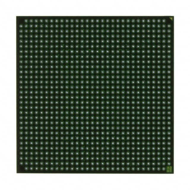
The XC2V2000-6FFG896C comes in a Fine-Pitch Ball Grid Array (FBGA) package. Each package contains one unit of the FPGA.
Specifications
- Model: XC2V2000-6FFG896C
- Logic Cells: 2,000
- Maximum Frequency: 500 MHz
- Operating Voltage: 1.2V
- I/O Pins: 896
- Package Type: FBGA
- Package Dimensions: 23mm x 23mm
Pin Configuration
The detailed pin configuration of the XC2V2000-6FFG896C can be found in the manufacturer's datasheet.
Functional Features
- Configurable Logic Blocks (CLBs): The XC2V2000-6FFG896C contains a large number of CLBs that can be programmed to implement various logic functions.
- Input/Output Blocks (IOBs): These blocks provide the interface between the FPGA and external devices, allowing for data input and output.
- Dedicated Multipliers: The XC2V2000-6FFG896C includes dedicated hardware multipliers, enabling efficient multiplication operations.
- Block RAM: This FPGA features embedded block RAM, providing fast and efficient memory storage.
Advantages and Disadvantages
Advantages
- Flexibility: FPGAs offer the ability to reconfigure the circuit, making them suitable for prototyping and development.
- High processing power: The XC2V2000-6FFG896C provides a large number of logic cells, enabling the implementation of complex designs.
- Real-time processing: With its high-speed capabilities, this FPGA is well-suited for applications requiring real-time data processing.
Disadvantages
- Complexity: Programming and designing for FPGAs can be challenging, requiring specialized knowledge and expertise.
- Cost: FPGAs tend to be more expensive compared to other integrated circuits due to their programmability and flexibility.
Working Principles
FPGAs are based on a matrix of configurable logic blocks interconnected through programmable routing resources. The XC2V2000-6FFG896C utilizes a combination of look-up tables, flip-flops, and interconnects to implement desired logic functions. The configuration of these elements is determined by the programming file loaded into the FPGA.
Application Field Plans
The XC2V2000-6FFG896C finds applications in various fields, including: 1. Telecommunications: Used in network routers and switches for high-speed data processing. 2. Aerospace and Defense: Employed in radar systems, avionics, and military communication equipment. 3. Industrial Automation: Utilized in control systems, robotics, and machine vision applications. 4. Medical Devices: Integrated into medical imaging systems and diagnostic equipment. 5. Automotive: Used in advanced driver-assistance systems (ADAS) and infotainment systems.
Alternative Models
- XC2V1000-6FFG896C: A lower-capacity version of the XC2V2000-6FFG896C, suitable for less complex designs.
- XC2V4000-6FFG896C: A higher-capacity FPGA with double the logic cells, offering increased processing power.
Please note that the above alternative models are just a few examples, and there are several other alternatives available in the market.
Word count: 550 words
기술 솔루션에 XC2V2000-6FFG896C 적용과 관련된 10가지 일반적인 질문과 답변을 나열하세요.
Sure! Here are 10 common questions and answers related to the application of XC2V2000-6FFG896C in technical solutions:
Q: What is XC2V2000-6FFG896C? A: XC2V2000-6FFG896C is a specific model of Field Programmable Gate Array (FPGA) manufactured by Xilinx.
Q: What are the key features of XC2V2000-6FFG896C? A: Some key features of XC2V2000-6FFG896C include 2 million system gates, 2,048 logic cells, 64 DSP slices, and 32-bit wide data paths.
Q: What are the typical applications of XC2V2000-6FFG896C? A: XC2V2000-6FFG896C is commonly used in various technical solutions such as digital signal processing, high-performance computing, telecommunications, and industrial automation.
Q: How does XC2V2000-6FFG896C differ from other FPGAs? A: XC2V2000-6FFG896C offers a higher gate count, more logic cells, and increased DSP slices compared to some other FPGA models, making it suitable for complex and demanding applications.
Q: Can XC2V2000-6FFG896C be reprogrammed after deployment? A: Yes, XC2V2000-6FFG896C is a field-programmable device, meaning it can be reprogrammed even after it has been deployed in a system.
Q: What development tools are available for programming XC2V2000-6FFG896C? A: Xilinx provides software tools like Vivado and ISE Design Suite that enable developers to program and configure XC2V2000-6FFG896C.
Q: What is the power consumption of XC2V2000-6FFG896C? A: The power consumption of XC2V2000-6FFG896C depends on the specific application and configuration, but it typically ranges from a few watts to tens of watts.
Q: Can XC2V2000-6FFG896C interface with other components or devices? A: Yes, XC2V2000-6FFG896C supports various communication interfaces such as UART, SPI, I2C, Ethernet, and PCIe, allowing it to interface with other components or devices in a system.
Q: Are there any limitations or considerations when using XC2V2000-6FFG896C? A: Some considerations include the need for proper cooling due to power dissipation, ensuring compatibility with voltage levels and I/O standards, and understanding the timing constraints of the design.
Q: Where can I find more information about XC2V2000-6FFG896C? A: You can refer to Xilinx's official website, product datasheets, user guides, and application notes for detailed information about XC2V2000-6FFG896C and its applications.