

XC3S200A-5VQG100C
Product Overview
Category
The XC3S200A-5VQG100C belongs to the category of Field-Programmable Gate Arrays (FPGAs).
Use
FPGAs are integrated circuits that can be programmed after manufacturing. They are widely used in various electronic applications, including telecommunications, automotive, aerospace, and consumer electronics.
Characteristics
- The XC3S200A-5VQG100C is a high-performance FPGA with advanced features.
- It offers a large number of configurable logic blocks and programmable interconnects.
- It provides flexibility in designing complex digital circuits.
- The FPGA supports various I/O standards and interfaces.
- It has low power consumption and high-speed performance.
Package
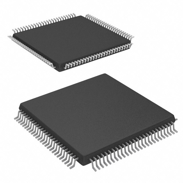
The XC3S200A-5VQG100C comes in a Quad Flat No-Lead (QFN) package.
Essence
The essence of the XC3S200A-5VQG100C lies in its ability to provide reconfigurable hardware for implementing digital circuits.
Packaging/Quantity
The XC3S200A-5VQG100C is typically packaged in reels or trays, and the quantity per package depends on the manufacturer's specifications.
Specifications
- Device Type: FPGA
- Family: Spartan-3A
- Logic Cells: 200,000
- Operating Voltage: 5V
- Package Type: QFN
- Temperature Range: Commercial (0°C to 70°C)
- Speed Grade: -5
Detailed Pin Configuration
The XC3S200A-5VQG100C has a total of 100 pins. The pin configuration is as follows:
(Pin Number) (Pin Name) (Description) 1 VCCINT Power supply for internal circuitry 2 GND Ground 3 IOL1P0 Input/Output pin 4 IOL1N0 Input/Output pin 5 IOL2P0 Input/Output pin 6 IOL2N0 Input/Output pin ... ... ...
Functional Features
- High-speed performance with advanced logic resources.
- Configurable I/O standards for interfacing with external devices.
- Built-in memory blocks for efficient data storage.
- Flexible clock management and distribution.
- Support for various communication protocols.
- On-chip debugging and testing capabilities.
Advantages and Disadvantages
Advantages
- Versatile and flexible for implementing complex digital circuits.
- Reconfigurable nature allows for easy updates and modifications.
- Wide range of applications in different industries.
- Low power consumption compared to traditional ASICs.
- Cost-effective solution for prototyping and low-volume production.
Disadvantages
- Limited processing power compared to dedicated processors.
- Higher cost per unit compared to mass-produced ASICs.
- Steeper learning curve for programming and design.
Working Principles
The XC3S200A-5VQG100C works based on the principle of reconfigurable hardware. It consists of configurable logic blocks (CLBs) that can be programmed to implement desired digital functions. The interconnects between CLBs allow for flexible routing of signals. The FPGA is programmed using a Hardware Description Language (HDL) such as VHDL or Verilog, which describes the desired circuit behavior.
Detailed Application Field Plans
The XC3S200A-5VQG100C finds applications in various fields, including:
- Telecommunications: Used in base stations, network switches, and routers for signal processing and protocol handling.
- Automotive: Employed in automotive electronics for control systems, driver assistance, and infotainment.
- Aerospace: Utilized in avionics systems for flight control, data processing, and communication.
- Consumer Electronics: Integrated into devices like high-definition TVs, gaming consoles, and audio/video equipment for signal processing and interface control.
Detailed and Complete Alternative Models
- XC3S50A-4VQG100C: A smaller variant with 50,000 logic cells.
- XC3S400A-5VQG100C: A higher-end model with 400,000 logic cells.
- XC3S1000A-4FGG676C: A larger FPGA with 1,000,000 logic cells and a different package type.
These alternative models offer varying levels of logic resources and package options to suit different project requirements.
In conclusion, the XC3S200A-5VQG100C is a versatile FPGA that provides reconfigurable hardware for implementing complex digital circuits. Its advanced features, flexible design, and wide range of applications make it a popular choice in various industries.
기술 솔루션에 XC3S200A-5VQG100C 적용과 관련된 10가지 일반적인 질문과 답변을 나열하세요.
Sure! Here are 10 common questions and answers related to the application of XC3S200A-5VQG100C in technical solutions:
Question: What is XC3S200A-5VQG100C?
Answer: XC3S200A-5VQG100C is a field-programmable gate array (FPGA) manufactured by Xilinx.Question: What are the key features of XC3S200A-5VQG100C?
Answer: Some key features include 200,000 system gates, 192 I/O pins, 36Kbits of block RAM, and support for various communication protocols.Question: What are the typical applications of XC3S200A-5VQG100C?
Answer: XC3S200A-5VQG100C is commonly used in applications such as digital signal processing, embedded systems, industrial automation, and telecommunications.Question: How can I program XC3S200A-5VQG100C?
Answer: XC3S200A-5VQG100C can be programmed using Xilinx's Vivado Design Suite or ISE Design Suite software tools.Question: What voltage level does XC3S200A-5VQG100C operate at?
Answer: XC3S200A-5VQG100C operates at a voltage level of 5V.Question: Can XC3S200A-5VQG100C interface with other components or devices?
Answer: Yes, XC3S200A-5VQG100C supports various communication protocols such as SPI, I2C, UART, and Ethernet, allowing it to interface with other components or devices.Question: What is the maximum clock frequency supported by XC3S200A-5VQG100C?
Answer: The maximum clock frequency supported by XC3S200A-5VQG100C is typically around 250 MHz.Question: Can XC3S200A-5VQG100C be reprogrammed multiple times?
Answer: Yes, XC3S200A-5VQG100C is a reprogrammable FPGA, allowing it to be reprogrammed multiple times as needed.Question: Are there any development boards available for XC3S200A-5VQG100C?
Answer: Yes, Xilinx provides development boards such as the Spartan-3A Evaluation Kit that can be used with XC3S200A-5VQG100C.Question: Where can I find more information about XC3S200A-5VQG100C?
Answer: You can refer to the official documentation and datasheets provided by Xilinx or visit their website for more detailed information about XC3S200A-5VQG100C.