

XC3S4000-4FGG900I
Product Overview
Category
XC3S4000-4FGG900I belongs to the category of Field Programmable Gate Arrays (FPGAs).
Use
FPGAs are integrated circuits that can be programmed and reprogrammed to perform various digital functions. They are widely used in industries such as telecommunications, automotive, aerospace, and consumer electronics.
Characteristics
XC3S4000-4FGG900I is a high-performance FPGA with advanced features. It offers flexibility, scalability, and reconfigurability, making it suitable for a wide range of applications.
Package
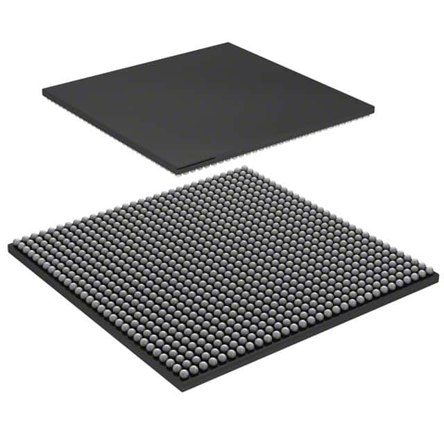
XC3S4000-4FGG900I comes in a compact package that ensures easy integration into electronic systems. The package type is FG900, which refers to a Fine-Pitch Ball Grid Array (BGA) package with 900 balls.
Essence
The essence of XC3S4000-4FGG900I lies in its ability to provide customizable digital logic functionality. It allows designers to implement complex digital circuits without the need for custom silicon solutions.
Packaging/Quantity
XC3S4000-4FGG900I is typically sold in reels or trays, depending on the manufacturer's packaging standards. The quantity per reel or tray may vary, but it is commonly available in quantities of 100 or more.
Specifications
- Device Type: FPGA
- Family: Spartan-3
- Series: XC3S
- Logic Cells: 4,000
- Speed Grade: -4
- Package Type: FG900
- Operating Temperature Range: -40°C to +85°C
- Supply Voltage: 1.2V
- I/O Voltage: 1.8V
- Number of I/Os: 900
- Configuration Memory: Non-volatile Flash
Detailed Pin Configuration
The XC3S4000-4FGG900I FPGA has a total of 900 pins, each serving a specific purpose. The pin configuration varies depending on the application requirements and the designer's implementation. For detailed pin assignments and configurations, please refer to the manufacturer's datasheet or user guide.
Functional Features
XC3S4000-4FGG900I offers several functional features that enhance its performance and usability:
- High Logic Capacity: With 4,000 logic cells, it can accommodate complex digital designs.
- Flexible I/O Options: The FPGA provides 900 I/O pins, allowing for versatile connectivity with external devices.
- Reconfigurability: The ability to reprogram the FPGA enables quick design iterations and system updates.
- Low Power Consumption: The device operates at a low supply voltage of 1.2V, resulting in energy-efficient operation.
- Advanced Clock Management: It supports various clocking options, including phase-locked loops (PLLs) for precise timing control.
Advantages and Disadvantages
Advantages
- Versatility: XC3S4000-4FGG900I can be used in a wide range of applications due to its flexibility and reconfigurability.
- Cost-Effective: FPGAs eliminate the need for custom ASIC development, reducing overall project costs.
- Rapid Prototyping: The ability to quickly modify and test designs accelerates the product development cycle.
Disadvantages
- Complexity: Designing with FPGAs requires specialized knowledge and expertise.
- Limited Performance: Compared to dedicated hardware solutions, FPGAs may have lower performance in certain applications.
- Higher Power Consumption: FPGAs consume more power compared to application-specific integrated circuits (ASICs).
Working Principles
XC3S4000-4FGG900I operates based on the principles of configurable logic. The FPGA consists of an array of programmable logic blocks interconnected through configurable routing resources. These logic blocks can be programmed to implement various digital functions, such as arithmetic operations, memory storage, and control logic. The configuration data is stored in non-volatile memory, allowing the FPGA to retain its functionality even after power cycles.
Detailed Application Field Plans
XC3S4000-4FGG900I finds applications in diverse fields, including:
- Telecommunications: Used in base stations, routers, and network switches for high-speed data processing and protocol handling.
- Automotive: Employed in advanced driver assistance systems (ADAS), infotainment systems, and engine control units (ECUs).
- Aerospace: Utilized in satellite communication systems, avionics, and flight control systems.
- Consumer Electronics: Integrated into smart TVs, gaming consoles, and wearable devices for enhanced performance and connectivity.
Detailed and Complete Alternative Models
There are several alternative models available in the market that offer similar functionality to XC3S4000-4FGG900I. Some notable alternatives include:
- Xilinx Spartan-6 FPGA Series
기술 솔루션에 XC3S4000-4FGG900I 적용과 관련된 10가지 일반적인 질문과 답변을 나열하세요.
Sure! Here are 10 common questions and answers related to the application of XC3S4000-4FGG900I in technical solutions:
Q: What is XC3S4000-4FGG900I? A: XC3S4000-4FGG900I is a field-programmable gate array (FPGA) manufactured by Xilinx. It is part of the Spartan-3 family and has 4000 logic cells.
Q: What are the key features of XC3S4000-4FGG900I? A: Some key features include a high-density programmable logic, on-chip RAM, multiple I/O standards, built-in clock management resources, and low power consumption.
Q: What are the typical applications of XC3S4000-4FGG900I? A: XC3S4000-4FGG900I can be used in various applications such as digital signal processing, telecommunications, industrial automation, aerospace, and defense.
Q: How can I program XC3S4000-4FGG900I? A: XC3S4000-4FGG900I can be programmed using Xilinx's Vivado Design Suite or ISE Design Suite software tools. These tools allow you to write and compile your design code and then program it onto the FPGA.
Q: What is the maximum operating frequency of XC3S4000-4FGG900I? A: The maximum operating frequency of XC3S4000-4FGG900I depends on the specific design and implementation. However, it can typically operate at frequencies up to several hundred megahertz.
Q: Can XC3S4000-4FGG900I interface with other components or devices? A: Yes, XC3S4000-4FGG900I supports various I/O standards such as LVCMOS, LVTTL, LVDS, and differential signaling. This allows it to interface with a wide range of components and devices.
Q: What is the power supply requirement for XC3S4000-4FGG900I? A: XC3S4000-4FGG900I requires a single 1.2V core voltage supply and a separate 2.5V or 3.3V auxiliary voltage supply for I/O banks.
Q: Can XC3S4000-4FGG900I be reprogrammed multiple times? A: Yes, XC3S4000-4FGG900I is a reprogrammable FPGA, which means you can program it multiple times with different designs or updates.
Q: Are there any development boards available for XC3S4000-4FGG900I? A: Yes, Xilinx provides development boards like the Spartan-3E Starter Kit that can be used for prototyping and testing designs based on XC3S4000-4FGG900I.
Q: Where can I find more information about XC3S4000-4FGG900I? A: You can find detailed information about XC3S4000-4FGG900I in the official documentation provided by Xilinx, including datasheets, user guides, and application notes.