

XC3S400A-4FG320C
Product Overview
Category
The XC3S400A-4FG320C belongs to the category of Field Programmable Gate Arrays (FPGAs).
Use
FPGAs are integrated circuits that can be programmed and reprogrammed to perform various digital functions. The XC3S400A-4FG320C is specifically designed for applications requiring high-performance logic capacity and flexibility.
Characteristics
- High-performance FPGA with 400,000 system gates
- Low power consumption
- Fast configuration and reconfiguration times
- Wide range of I/O standards and interfaces
- Support for advanced features like embedded memory blocks and DSP slices
Package
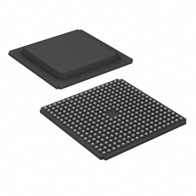
The XC3S400A-4FG320C comes in a compact FG320 package, which refers to the number of pins and the specific pin arrangement on the chip.
Essence
The essence of the XC3S400A-4FG320C lies in its ability to provide a customizable hardware platform for implementing complex digital designs. It offers designers the flexibility to create tailored solutions for a wide range of applications.
Packaging/Quantity
The XC3S400A-4FG320C is typically packaged in trays or reels, depending on the quantity ordered. The exact packaging and quantity may vary based on customer requirements.
Specifications
- Logic Cells: 400,000
- System Gates: 400,000
- Block RAM: 1,152 Kbits
- DSP Slices: 192
- Maximum I/O Pins: 320
- Operating Voltage: 1.2V
- Operating Temperature Range: -40°C to +100°C
Detailed Pin Configuration
The XC3S400A-4FG320C has a total of 320 pins, each serving a specific purpose in the overall functionality of the FPGA. The detailed pin configuration can be found in the product datasheet.
Functional Features
1. High Logic Capacity
With 400,000 logic cells and system gates, the XC3S400A-4FG320C offers ample resources for implementing complex digital designs.
2. Flexible I/O Standards
The FPGA supports a wide range of I/O standards, allowing seamless integration with various external devices and interfaces.
3. Fast Configuration Time
The XC3S400A-4FG320C features fast configuration and reconfiguration times, enabling rapid prototyping and development cycles.
4. Advanced Features
Embedded memory blocks and DSP slices provide additional functionality for applications requiring high-speed data processing and storage.
Advantages and Disadvantages
Advantages
- High logic capacity for complex designs
- Flexible I/O standards for easy integration
- Fast configuration time for rapid development
- Support for advanced features like embedded memory and DSP
Disadvantages
- Relatively higher power consumption compared to other low-power alternatives
- Limited availability of alternative models with similar specifications
Working Principles
The XC3S400A-4FG320C operates based on the principles of reconfigurable computing. It consists of an array of configurable logic blocks interconnected through programmable routing resources. The user programs the FPGA using a Hardware Description Language (HDL) or a graphical design tool, defining the desired functionality and interconnections.
Once programmed, the FPGA executes the specified digital functions by routing signals through the configured logic blocks and interconnects. This flexibility allows for the implementation of a wide range of applications.
Detailed Application Field Plans
The XC3S400A-4FG320C finds applications in various fields, including:
- Communications: Used in wireless base stations, routers, and network switches for signal processing and protocol handling.
- Industrial Automation: Employed in control systems, motor drives, and robotics for real-time control and monitoring.
- Aerospace and Defense: Utilized in radar systems, avionics, and secure communication equipment for high-performance signal processing and encryption.
- Medical Devices: Integrated into medical imaging systems, patient monitoring devices, and diagnostic equipment for data acquisition and processing.
Detailed and Complete Alternative Models
While the XC3S400A-4FG320C offers a unique combination of features and specifications, alternative models with similar capabilities include:
- XC3S500E-4PQG208C
- XC3S1000-4FG456C
- XC3S2000-4FG676C
These alternatives provide varying logic capacities, package options, and pin configurations to cater to different application requirements.
In conclusion, the XC3S400A-4FG320C is a high-performance FPGA that offers flexibility, advanced features, and a wide range of applications. Its customizable nature and extensive resources make it an ideal choice for designers seeking to implement complex digital designs.
기술 솔루션에 XC3S400A-4FG320C 적용과 관련된 10가지 일반적인 질문과 답변을 나열하세요.
Sure! Here are 10 common questions and answers related to the application of XC3S400A-4FG320C in technical solutions:
Question: What is XC3S400A-4FG320C?
- Answer: XC3S400A-4FG320C is a specific model of Field-Programmable Gate Array (FPGA) manufactured by Xilinx.Question: What are the key features of XC3S400A-4FG320C?
- Answer: Some key features include 400,000 system gates, 400 MHz performance, 320-pin Fine-Pitch Ball Grid Array (FBGA) package, and 4ns minimum clock-to-output delay.Question: In what applications can XC3S400A-4FG320C be used?
- Answer: XC3S400A-4FG320C can be used in various applications such as digital signal processing, telecommunications, industrial automation, aerospace, and more.Question: How does XC3S400A-4FG320C differ from other FPGA models?
- Answer: XC3S400A-4FG320C has its own unique combination of gate count, performance, and package size, which makes it suitable for specific applications.Question: Can XC3S400A-4FG320C be programmed after installation?
- Answer: Yes, XC3S400A-4FG320C is a Field-Programmable device, meaning it can be reprogrammed even after being installed in a system.Question: What programming languages can be used with XC3S400A-4FG320C?
- Answer: XC3S400A-4FG320C can be programmed using Hardware Description Languages (HDLs) such as VHDL or Verilog.Question: Are there any development tools available for XC3S400A-4FG320C?
- Answer: Yes, Xilinx provides development tools like Vivado Design Suite that can be used to design, simulate, and program XC3S400A-4FG320C.Question: Can XC3S400A-4FG320C interface with other components in a system?
- Answer: Yes, XC3S400A-4FG320C has various I/O pins that can be used to interface with other components such as sensors, memory devices, communication modules, etc.Question: What is the power supply requirement for XC3S400A-4FG320C?
- Answer: XC3S400A-4FG320C typically requires a 1.2V core voltage and a 3.3V auxiliary voltage for proper operation.Question: Where can I find more information about XC3S400A-4FG320C?
- Answer: You can refer to the official documentation provided by Xilinx, including datasheets, user guides, and application notes, for detailed information about XC3S400A-4FG320C.