

XC3S500E-5PQ208C
Product Overview
Category
The XC3S500E-5PQ208C belongs to the category of Field-Programmable Gate Arrays (FPGAs).
Use
This product is primarily used in digital logic circuits for various applications such as telecommunications, automotive, industrial automation, and consumer electronics.
Characteristics
- High-performance FPGA with advanced features
- Low power consumption
- Flexible and reconfigurable design
- Large number of programmable logic cells
- Integrated memory blocks
- Support for various communication protocols
- High-speed data processing capabilities
Package
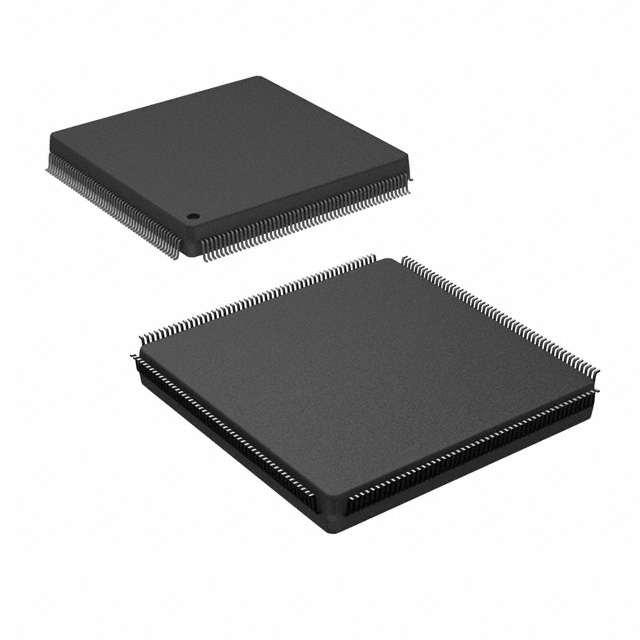
The XC3S500E-5PQ208C comes in a PQ208 package, which refers to a plastic quad flat pack with 208 pins.
Essence
The essence of this product lies in its ability to provide a customizable and versatile solution for implementing complex digital systems. It allows designers to create their own digital circuits by programming the FPGA according to their specific requirements.
Packaging/Quantity
The XC3S500E-5PQ208C is typically packaged in reels or trays, depending on the manufacturer's specifications. The quantity per reel or tray may vary, but it is commonly available in quantities of 250 or 500 units.
Specifications
- FPGA Family: Spartan-3E
- Logic Cells: 5,136
- Flip-Flops: 10,272
- Block RAM: 360 Kb
- Maximum Frequency: 500 MHz
- I/O Pins: 208
- Operating Voltage: 1.2V
- Operating Temperature Range: -40°C to +85°C
Detailed Pin Configuration
The XC3S500E-5PQ208C has a total of 208 pins, each serving a specific purpose in the overall functionality of the FPGA. The pin configuration includes input/output pins, power supply pins, clock pins, and configuration pins. For a detailed pinout diagram, please refer to the product datasheet.
Functional Features
- Configurable logic blocks for implementing custom digital circuits
- Dedicated hardware multipliers for efficient arithmetic operations
- Built-in memory blocks for data storage and retrieval
- Programmable I/O interfaces supporting various standards (e.g., LVCMOS, LVTTL, LVDS)
- Clock management resources for precise timing control
- On-chip configuration memory for storing FPGA programming bitstreams
Advantages and Disadvantages
Advantages
- Flexibility: The XC3S500E-5PQ208C allows designers to create highly customized digital circuits tailored to their specific requirements.
- Reconfigurability: The FPGA can be reprogrammed multiple times, enabling iterative design improvements and adaptability to changing system needs.
- High Performance: With its advanced features and high-speed data processing capabilities, this FPGA offers excellent performance for demanding applications.
Disadvantages
- Complexity: Designing and programming an FPGA requires specialized knowledge and expertise, making it more challenging compared to using pre-designed integrated circuits.
- Cost: FPGAs tend to be more expensive than off-the-shelf integrated circuits due to their flexibility and customization capabilities.
Working Principles
The XC3S500E-5PQ208C operates based on the principles of configurable logic. It consists of an array of programmable logic cells interconnected through configurable routing resources. These logic cells can be programmed to implement various digital functions, such as logic gates, multiplexers, and flip-flops. The interconnections between these cells are determined by the user's design, allowing for the creation of complex digital systems.
Detailed Application Field Plans
The XC3S500E-5PQ208C finds applications in a wide range of fields, including:
- Telecommunications: Used in base stations, network switches, and routers for high-speed data processing and protocol handling.
- Automotive: Employed in automotive control systems, infotainment systems, and driver assistance systems for real-time data processing and control.
- Industrial Automation: Utilized in programmable logic controllers (PLCs), motor control systems, and industrial monitoring equipment for precise control and data acquisition.
- Consumer Electronics: Integrated into smart TVs, gaming consoles, and multimedia devices for enhanced performance and functionality.
Detailed and Complete Alternative Models
- XC3S100E-4VQG100C: A smaller variant of the same FPGA family with 100,000 system gates and 100 pins.
- XC3S200E-4FT256C: A higher-capacity FPGA with 200,000 system gates and 256 pins.
- XC3S400E-5FGG320C: A larger FPGA with 400,000 system gates and 320 pins.
These alternative models offer varying capacities and pin counts to cater to different design requirements.
In conclusion, the XC3S500E-5
기술 솔루션에 XC3S500E-5PQ208C 적용과 관련된 10가지 일반적인 질문과 답변을 나열하세요.
Sure! Here are 10 common questions and answers related to the application of XC3S500E-5PQ208C in technical solutions:
Question: What is XC3S500E-5PQ208C?
Answer: XC3S500E-5PQ208C is a field-programmable gate array (FPGA) from Xilinx, which offers programmable logic and digital signal processing capabilities.Question: What are the key features of XC3S500E-5PQ208C?
Answer: Some key features of XC3S500E-5PQ208C include 500K system gates, 36K logic cells, 18 multipliers, 4 digital clock managers, and various I/O options.Question: What are the typical applications of XC3S500E-5PQ208C?
Answer: XC3S500E-5PQ208C is commonly used in applications such as industrial automation, telecommunications, automotive electronics, medical devices, and aerospace systems.Question: How can XC3S500E-5PQ208C be programmed?
Answer: XC3S500E-5PQ208C can be programmed using Xilinx's Vivado Design Suite or ISE Design Suite software tools.Question: What programming languages can be used with XC3S500E-5PQ208C?
Answer: XC3S500E-5PQ208C supports various hardware description languages (HDLs) such as VHDL and Verilog for designing and programming the FPGA.Question: Can XC3S500E-5PQ208C interface with other components or devices?
Answer: Yes, XC3S500E-5PQ208C has multiple I/O options, including GPIO pins, serial interfaces (SPI, I2C, UART), and high-speed transceivers, allowing it to interface with other components or devices.Question: What are the power requirements for XC3S500E-5PQ208C?
Answer: XC3S500E-5PQ208C typically operates at a voltage range of 1.14V to 1.26V, with additional power supply pins for I/O banks and configuration.Question: Can XC3S500E-5PQ208C be reprogrammed multiple times?
Answer: Yes, XC3S500E-5PQ208C is a reprogrammable FPGA, which means it can be programmed and reprogrammed multiple times as per the application requirements.Question: Are there any development boards available for XC3S500E-5PQ208C?
Answer: Yes, Xilinx offers development boards like the Spartan-3E Starter Kit, which provide a platform for prototyping and testing designs using XC3S500E-5PQ208C.Question: Where can I find technical documentation and support for XC3S500E-5PQ208C?
Answer: You can find technical documentation, datasheets, application notes, and support resources on Xilinx's official website or community forums dedicated to FPGA development.