

XC4008E-1PC84C
Product Overview
Category
XC4008E-1PC84C belongs to the category of programmable logic devices (PLDs).
Use
This product is used in digital circuit design and implementation. It provides a flexible and customizable solution for various applications.
Characteristics
- Programmable: The XC4008E-1PC84C can be programmed to perform specific functions according to the user's requirements.
- High Integration: It integrates multiple logic gates, flip-flops, and other components into a single device, reducing the need for external components.
- Versatile: It can be used in a wide range of applications, including telecommunications, automotive, industrial control, and consumer electronics.
- Low Power Consumption: The XC4008E-1PC84C is designed to operate efficiently with low power consumption.
- Fast Operation: It offers high-speed performance, enabling quick execution of complex logic operations.
Package and Quantity
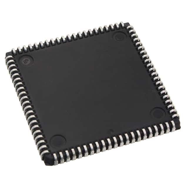
The XC4008E-1PC84C is available in a 84-pin plastic package. Each package contains one unit of the device.
Specifications
- Logic Cells: 4008
- Maximum Operating Frequency: 100 MHz
- Input/Output Pins: 84
- Supply Voltage: 3.3V
- Operating Temperature Range: -40°C to 85°C
Pin Configuration
The detailed pin configuration of XC4008E-1PC84C can be found in the datasheet provided by the manufacturer.
Functional Features
- Programmable Logic: The XC4008E-1PC84C allows users to program the device to implement desired logic functions.
- Flip-Flops: It includes built-in flip-flops that can store and manipulate binary data.
- I/O Interfaces: The device provides input/output interfaces for communication with external components.
- Clock Management: It supports clock signals for synchronous operation.
- Memory: The XC4008E-1PC84C includes on-chip memory elements for data storage.
Advantages
- Flexibility: The programmable nature of XC4008E-1PC84C allows for easy customization and adaptation to changing requirements.
- Cost-Effective: By eliminating the need for multiple discrete components, it reduces overall system cost.
- Time-Saving: The device simplifies the design process by providing a ready-to-use solution that can be quickly programmed.
Disadvantages
- Complexity: Programming and configuring the XC4008E-1PC84C may require specialized knowledge and expertise.
- Limited Resources: The device has a finite number of logic cells and I/O pins, which may restrict the complexity of designs.
Working Principles
The XC4008E-1PC84C operates based on the principles of digital logic. It utilizes configurable logic blocks (CLBs) and interconnect resources to implement user-defined logic functions. These CLBs consist of look-up tables (LUTs), flip-flops, and other components that can be interconnected to create complex digital circuits.
Application Field Plans
The XC4008E-1PC84C finds applications in various fields, including: - Telecommunications: It can be used in communication systems for signal processing, protocol implementation, and error correction. - Automotive: The device is suitable for automotive electronics, such as engine control units, infotainment systems, and driver assistance systems. - Industrial Control: It enables the implementation of control systems for industrial automation, robotics, and monitoring. - Consumer Electronics: The XC4008E-1PC84C can be utilized in devices like gaming consoles, home appliances, and audio/video equipment.
Alternative Models
- XC4008E-2PC84C: Similar to XC4008E-1PC84C but with enhanced specifications.
- XC4008E-1FG676C: A different package variant of XC4008E-1PC84C with 676 pins.
In conclusion, the XC4008E-1PC84C is a programmable logic device that offers flexibility, high integration, and low power consumption. It finds applications in various fields and provides advantages such as cost-effectiveness and time-saving. However, it may require specialized knowledge for programming and has limitations in terms of resources.
기술 솔루션에 XC4008E-1PC84C 적용과 관련된 10가지 일반적인 질문과 답변을 나열하세요.
Sure! Here are 10 common questions and answers related to the application of XC4008E-1PC84C in technical solutions:
Q1: What is XC4008E-1PC84C? A1: XC4008E-1PC84C is a specific model of Field Programmable Gate Array (FPGA) manufactured by Xilinx.
Q2: What are the key features of XC4008E-1PC84C? A2: Some key features of XC4008E-1PC84C include 4000 logic cells, 8 input/output blocks, 84-pin plastic package, and support for various I/O standards.
Q3: What are the typical applications of XC4008E-1PC84C? A3: XC4008E-1PC84C can be used in a wide range of applications such as digital signal processing, telecommunications, industrial control systems, and embedded systems.
Q4: How does XC4008E-1PC84C differ from other FPGA models? A4: XC4008E-1PC84C has its own unique combination of logic cells, I/O blocks, and package size, which makes it suitable for specific design requirements.
Q5: What programming languages can be used with XC4008E-1PC84C? A5: XC4008E-1PC84C can be programmed using Hardware Description Languages (HDLs) such as VHDL or Verilog.
Q6: Can XC4008E-1PC84C be reprogrammed after initial configuration? A6: Yes, XC4008E-1PC84C is a reprogrammable FPGA, allowing for flexibility in design iterations and updates.
Q7: What tools are available for designing with XC4008E-1PC84C? A7: Xilinx provides software tools like Vivado or ISE Design Suite that enable designers to create, simulate, and program XC4008E-1PC84C.
Q8: What are the power requirements for XC4008E-1PC84C? A8: The power requirements for XC4008E-1PC84C typically include a supply voltage of 3.3V or 5V, depending on the specific design requirements.
Q9: Can XC4008E-1PC84C interface with other components or devices? A9: Yes, XC4008E-1PC84C can interface with other components or devices through its I/O blocks, supporting various communication protocols such as SPI, I2C, UART, etc.
Q10: Are there any limitations or considerations when using XC4008E-1PC84C? A10: Some considerations include the available logic resources, I/O pin count, power consumption, and timing constraints that need to be taken into account during the design process.
Please note that these questions and answers are general in nature and may vary based on specific design requirements and application scenarios.