

XC4008E-2PC84I
Product Overview
Category
XC4008E-2PC84I belongs to the category of programmable logic devices (PLDs).
Use
This product is commonly used in digital circuit design and implementation. It provides a flexible and customizable solution for various applications.
Characteristics
- Programmable: The XC4008E-2PC84I can be programmed to perform specific functions according to the user's requirements.
- High Integration: This device integrates multiple logic gates, flip-flops, and other components into a single chip.
- Versatile: It supports a wide range of applications due to its programmability.
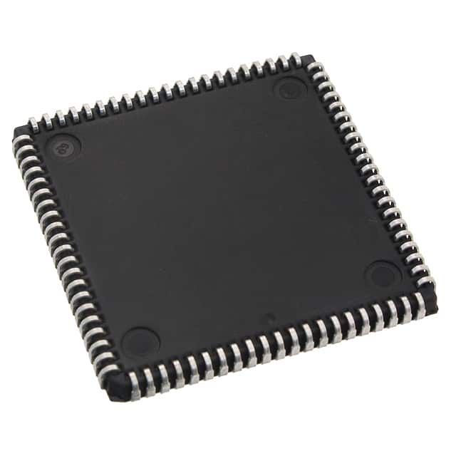
- Compact Package: The XC4008E-2PC84I comes in a 84-pin plastic package, which ensures easy handling and installation.
Packaging/Quantity
The XC4008E-2PC84I is typically packaged in a plastic tray or tube. The quantity per package may vary depending on the manufacturer, but it is usually sold in quantities of 1 to 10 units.
Specifications
- Logic Cells: 4008
- Maximum Operating Frequency: 100 MHz
- Number of I/O Pins: 68
- Supply Voltage: 3.3V
- Operating Temperature Range: -40°C to 85°C
Detailed Pin Configuration
The XC4008E-2PC84I has a total of 84 pins. Here is a brief overview of the pin configuration:
- Pin 1: VCCIO - Power supply for I/O buffers
- Pin 2: GND - Ground
- Pin 3: TCK - Test clock input
- Pin 4: TMS - Test mode select input
- Pin 5: TDI - Test data input
- Pin 6: TDO - Test data output
- ...
- Pin 84: VCC - Power supply for core logic
For a complete pin configuration diagram, please refer to the product datasheet.
Functional Features
- Programmable Logic: The XC4008E-2PC84I offers a wide range of programmable logic elements, allowing users to implement complex digital circuits.
- Flip-Flops: It includes a number of flip-flops that can be used for sequential logic design.
- I/O Buffers: The device provides input/output buffers for interfacing with external devices.
- Clock Management: It supports clock signals for synchronous operation.
Advantages and Disadvantages
Advantages
- Flexibility: The programmability of XC4008E-2PC84I allows for easy customization and modification of circuit designs.
- Integration: It integrates multiple components into a single chip, reducing the overall size and complexity of the system.
- Versatility: This device can be used in various applications due to its wide range of programmable features.
Disadvantages
- Complexity: Programming and configuring the XC4008E-2PC84I may require specialized knowledge and expertise.
- Limited Resources: The number of logic cells and I/O pins may not be sufficient for highly complex designs.
Working Principles
The XC4008E-2PC84I operates based on the principles of programmable logic. It consists of an array of configurable logic blocks (CLBs) interconnected through programmable interconnects. These CLBs can be programmed to perform specific logic functions, such as AND, OR, and XOR gates, as well as flip-flops for sequential logic.
The device is programmed using hardware description languages (HDL) or schematic entry tools. Once programmed, it can execute the desired logic functions based on the input signals provided.
Detailed Application Field Plans
The XC4008E-2PC84I finds applications in various fields, including:
- Communications: It can be used in the design of communication systems, such as routers and switches.
- Industrial Automation: This device is suitable for implementing control logic in industrial automation systems.
- Consumer Electronics: It can be utilized in the development of consumer electronic devices, such as gaming consoles and multimedia players.
- Automotive: The XC4008E-2PC84I can be employed in automotive applications, including engine control units and infotainment systems.
Detailed and Complete Alternative Models
- XC4008E-3PC84I: Similar to XC4008E-2PC84I, but with enhanced performance and additional features.
- XC4008EX-2PC84I: A higher-end version of XC4008E-2PC84I, offering increased logic capacity and faster operating frequency.
- XC4008XL-2PC84I: An alternative model with extended functionality and improved power efficiency.
These alternative models provide users with a range of options based on their specific requirements and project needs.
In conclusion, the XC4008E-2PC84I is a programmable logic device that
기술 솔루션에 XC4008E-2PC84I 적용과 관련된 10가지 일반적인 질문과 답변을 나열하세요.
Sure! Here are 10 common questions and answers related to the application of XC4008E-2PC84I in technical solutions:
Q: What is XC4008E-2PC84I? A: XC4008E-2PC84I is a specific model of Field Programmable Gate Array (FPGA) manufactured by Xilinx.
Q: What are the key features of XC4008E-2PC84I? A: Some key features of XC4008E-2PC84I include 4000 gates, 84-pin plastic package, and 2.5V power supply.
Q: How can XC4008E-2PC84I be used in technical solutions? A: XC4008E-2PC84I can be used for various applications such as digital signal processing, embedded systems, and high-performance computing.
Q: What programming languages are supported by XC4008E-2PC84I? A: XC4008E-2PC84I can be programmed using Hardware Description Languages (HDLs) like VHDL or Verilog.
Q: Can XC4008E-2PC84I be reprogrammed after initial configuration? A: Yes, XC4008E-2PC84I is a reprogrammable FPGA, allowing for flexibility in design changes.
Q: What tools are available for designing with XC4008E-2PC84I? A: Xilinx provides software tools like Vivado Design Suite that support the design and implementation of XC4008E-2PC84I-based solutions.
Q: Are there any limitations to consider when using XC4008E-2PC84I? A: XC4008E-2PC84I has a limited number of gates and pins, so larger designs may require higher-capacity FPGAs.
Q: Can XC4008E-2PC84I interface with other components or devices? A: Yes, XC4008E-2PC84I can interface with various peripherals and devices through its I/O pins.
Q: What is the power consumption of XC4008E-2PC84I? A: The power consumption of XC4008E-2PC84I depends on the design and operating conditions but typically falls within a specified range provided in the datasheet.
Q: Where can I find more information about XC4008E-2PC84I? A: More detailed information about XC4008E-2PC84I can be found in the Xilinx product documentation, including datasheets and user guides.
Please note that the answers provided here are general and may vary depending on specific requirements and use cases.