

XC4VLX100-12FFG1148C
Product Overview
Category
XC4VLX100-12FFG1148C belongs to the category of Field Programmable Gate Arrays (FPGAs).
Use
FPGAs are integrated circuits that can be programmed and reprogrammed to perform various digital functions. They are widely used in industries such as telecommunications, automotive, aerospace, and consumer electronics.
Characteristics
XC4VLX100-12FFG1148C is known for its high performance and versatility. It offers a large number of programmable logic cells, abundant memory resources, and flexible I/O options. These characteristics make it suitable for complex digital designs and applications requiring real-time processing.
Package
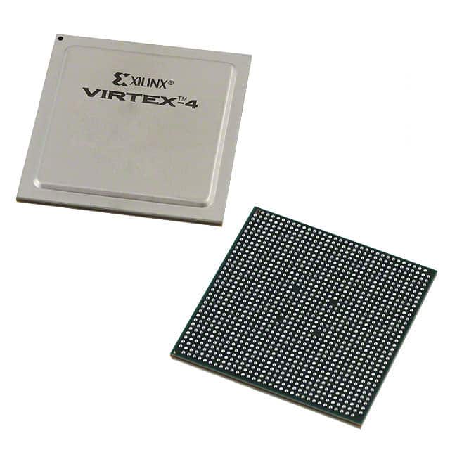
XC4VLX100-12FFG1148C is available in a 1148-ball Fine-Pitch Ball Grid Array (FBGA) package. This package provides a compact form factor and excellent thermal performance.
Essence
The essence of XC4VLX100-12FFG1148C lies in its ability to provide a customizable hardware platform that can be tailored to specific application requirements. Its programmability allows designers to implement complex algorithms and functions in hardware, resulting in improved performance and reduced time-to-market.
Packaging/Quantity
XC4VLX100-12FFG1148C is typically sold in trays or reels, with each containing a specific quantity of devices. The exact packaging and quantity may vary depending on the supplier.
Specifications
- FPGA Family: Virtex-4 LX
- Logic Cells: 100,000
- System Gates: 200,000
- Block RAM: 2,592 Kbits
- DSP Slices: 192
- Maximum Frequency: 400 MHz
- Operating Voltage: 1.2V
- I/O Standards: LVCMOS, LVTTL, LVDS, HSTL, SSTL
Detailed Pin Configuration
The XC4VLX100-12FFG1148C FPGA has a total of 1148 pins. These pins are assigned to various functions such as input/output (I/O) signals, clock inputs, configuration interfaces, and power supply connections. A detailed pinout diagram and description can be found in the device's datasheet.
Functional Features
XC4VLX100-12FFG1148C offers several functional features that enhance its performance and usability:
- High Logic Capacity: With 100,000 logic cells and 200,000 system gates, it can accommodate complex designs.
- Abundant Memory Resources: The 2,592 Kbits of block RAM provide ample storage for data-intensive applications.
- Flexible I/O Options: The FPGA supports various I/O standards, allowing seamless integration with different external devices.
- DSP Slices: The 192 dedicated Digital Signal Processing (DSP) slices enable efficient implementation of signal processing algorithms.
Advantages and Disadvantages
Advantages
- Flexibility: FPGAs offer the advantage of reprogrammability, allowing designers to adapt their designs to changing requirements.
- High Performance: XC4VLX100-12FFG1148C provides high-speed processing capabilities, making it suitable for demanding applications.
- Time-to-Market: By using FPGAs, designers can reduce development time and quickly prototype their designs.
- Cost-Effective: FPGAs eliminate the need for custom ASICs, reducing manufacturing costs for low to medium volume production.
Disadvantages
- Power Consumption: FPGAs tend to consume more power compared to fixed-function integrated circuits.
- Complexity: Designing with FPGAs requires specialized knowledge and expertise, which may pose challenges for inexperienced designers.
- Limited Resources: Despite their high capacity, FPGAs have finite resources, and complex designs may require larger devices.
Working Principles
XC4VLX100-12FFG1148C operates based on the principles of configurable logic. The FPGA consists of an array of programmable logic cells interconnected through configurable routing resources. These logic cells can be programmed to implement various digital functions by configuring the interconnections and functionality of the individual cells.
During operation, the FPGA is configured with a bitstream that defines the desired functionality. This configuration data is stored in non-volatile memory or loaded dynamically at startup. Once configured, the FPGA executes the desired logic functions, processing input signals and generating output signals according to the programmed design.
Detailed Application Field Plans
XC4VLX100-12FFG1148C finds applications in a wide range of fields, including:
- Telecommunications: Used in base stations, routers, and network switches for high-speed data processing.
- Automotive: Employed in advanced driver-assistance systems (ADAS) for real-time image processing and sensor fusion.
- Aerospace: Utilized in satellite communication systems, radar signal
기술 솔루션에 XC4VLX100-12FFG1148C 적용과 관련된 10가지 일반적인 질문과 답변을 나열하세요.
Sure! Here are 10 common questions and answers related to the application of XC4VLX100-12FFG1148C in technical solutions:
Q: What is XC4VLX100-12FFG1148C? A: XC4VLX100-12FFG1148C is a field-programmable gate array (FPGA) manufactured by Xilinx.
Q: What are the key features of XC4VLX100-12FFG1148C? A: Some key features include 100,000 logic cells, 12ns maximum delay, and 1.2V core voltage.
Q: What applications can XC4VLX100-12FFG1148C be used for? A: XC4VLX100-12FFG1148C can be used in various applications such as telecommunications, industrial automation, and aerospace.
Q: How does XC4VLX100-12FFG1148C differ from other FPGAs? A: XC4VLX100-12FFG1148C offers higher logic capacity, faster performance, and lower power consumption compared to some other FPGAs.
Q: Can XC4VLX100-12FFG1148C be reprogrammed after deployment? A: Yes, XC4VLX100-12FFG1148C is a field-programmable device, meaning it can be reprogrammed even after it has been deployed in a system.
Q: What development tools are available for programming XC4VLX100-12FFG1148C? A: Xilinx provides software tools like Vivado Design Suite that allow developers to program and configure XC4VLX100-12FFG1148C.
Q: What is the power consumption of XC4VLX100-12FFG1148C? A: The power consumption of XC4VLX100-12FFG1148C depends on the specific design and usage, but it typically operates at low power levels.
Q: Can XC4VLX100-12FFG1148C interface with other components or devices? A: Yes, XC4VLX100-12FFG1148C supports various interfaces such as GPIO, UART, SPI, I2C, Ethernet, and more, allowing it to communicate with other components or devices.
Q: Are there any limitations or considerations when using XC4VLX100-12FFG1148C? A: Some considerations include power supply requirements, thermal management, and ensuring proper signal integrity in high-speed designs.
Q: Where can I find additional resources or support for XC4VLX100-12FFG1148C? A: Xilinx provides documentation, application notes, forums, and technical support to assist users in designing and implementing solutions with XC4VLX100-12FFG1148C.
Please note that the specific details and answers may vary depending on the context and requirements of your technical solution.