

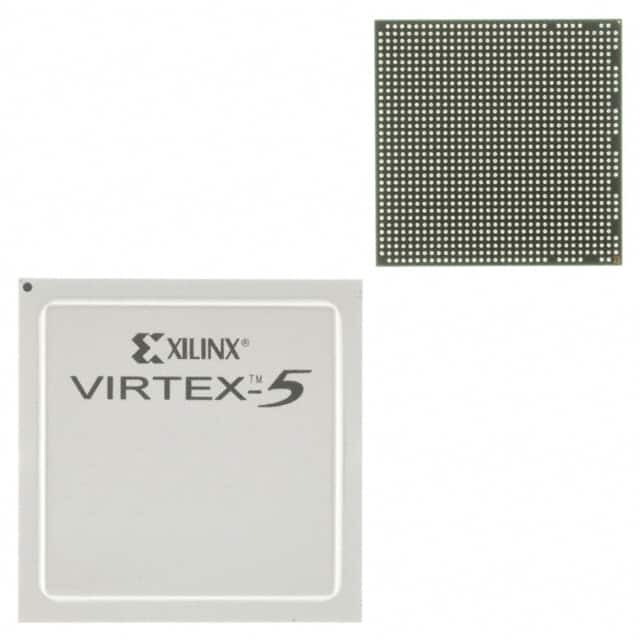
XC5VLX50-2FF1153C
Product Overview
Category
The XC5VLX50-2FF1153C belongs to the category of Field Programmable Gate Arrays (FPGAs).
Use
FPGAs are integrated circuits that can be programmed and reprogrammed to perform various digital functions. The XC5VLX50-2FF1153C is specifically designed for high-performance applications.
Characteristics
- High-performance FPGA with advanced features
- Flexible and reprogrammable design
- Suitable for complex digital systems
- Offers high-speed data processing capabilities
Package
The XC5VLX50-2FF1153C comes in a specific package, which ensures its physical protection and facilitates its integration into electronic systems.
Essence
The essence of the XC5VLX50-2FF1153C lies in its ability to provide a customizable and high-performance solution for digital system designs.
Packaging/Quantity
The XC5VLX50-2FF1153C is typically packaged individually and is available in varying quantities depending on the requirements of the user.
Specifications
- FPGA Family: Virtex-5
- Logic Cells: 48,576
- Number of I/Os: 256
- Operating Voltage: 1.2V
- Speed Grade: -2
- Package Type: FF1153
Detailed Pin Configuration
The XC5VLX50-2FF1153C has a specific pin configuration that allows for the connection of various input and output signals. The detailed pin configuration can be found in the product datasheet.
Functional Features
The XC5VLX50-2FF1153C offers several functional features that make it suitable for a wide range of applications:
- High-speed data processing capabilities
- Configurable logic cells for custom digital circuit implementation
- Integrated memory blocks for efficient data storage
- Flexible I/O interfaces for seamless integration with external devices
- On-chip clock management resources for precise timing control
Advantages and Disadvantages
Advantages
- High-performance FPGA suitable for complex digital systems
- Reprogrammable design allows for flexibility in system development
- Offers a wide range of functional features for diverse applications
- Efficient use of resources for optimized power consumption
Disadvantages
- Requires expertise in FPGA programming for effective utilization
- Relatively higher cost compared to other digital logic solutions
- Limited availability of alternative models with similar specifications
Working Principles
The XC5VLX50-2FF1153C operates based on the principles of reconfigurable computing. It consists of configurable logic cells, memory blocks, and I/O interfaces that can be programmed to implement custom digital circuits. The FPGA's internal routing resources allow for the interconnection of these components, enabling the desired functionality.
Detailed Application Field Plans
The XC5VLX50-2FF1153C finds applications in various fields, including:
- Telecommunications: Used in high-speed data processing applications such as network routers and switches.
- Aerospace and Defense: Employed in radar systems, avionics, and secure communication equipment.
- Industrial Automation: Utilized for real-time control and monitoring in manufacturing processes.
- Medical Devices: Integrated into medical imaging systems and diagnostic equipment.
- Research and Development: Used in prototyping and testing of digital designs.
Detailed and Complete Alternative Models
While the XC5VLX50-2FF1153C offers specific features and capabilities, there are alternative models available from other FPGA manufacturers. Some notable alternatives include:
- Altera Cyclone V series
- Lattice ECP5 series
- Xilinx Spartan-6 series
These alternative models provide similar functionalities and can be considered based on specific project requirements.
In conclusion, the XC5VLX50-2FF1153C is a high-performance FPGA belonging to the Virtex-5 family. It offers flexibility, advanced features, and high-speed data processing capabilities for various applications in telecommunications, aerospace, industrial automation, medical devices, and research. While it has advantages such as reprogrammability and resource efficiency, it requires expertise in FPGA programming and may have limited availability of alternative models with similar specifications.
기술 솔루션에 XC5VLX50-2FF1153C 적용과 관련된 10가지 일반적인 질문과 답변을 나열하세요.
Sure! Here are 10 common questions and answers related to the application of XC5VLX50-2FF1153C in technical solutions:
Question: What is XC5VLX50-2FF1153C?
- Answer: XC5VLX50-2FF1153C is a field-programmable gate array (FPGA) from Xilinx, which is commonly used in various technical solutions.Question: What are the key features of XC5VLX50-2FF1153C?
- Answer: Some key features of XC5VLX50-2FF1153C include 50,000 logic cells, 1,153 I/O pins, 2.5V core voltage, and support for various communication protocols.Question: In what applications can XC5VLX50-2FF1153C be used?
- Answer: XC5VLX50-2FF1153C can be used in a wide range of applications such as telecommunications, industrial automation, aerospace, defense, and high-performance computing.Question: What programming languages can be used with XC5VLX50-2FF1153C?
- Answer: XC5VLX50-2FF1153C can be programmed using hardware description languages (HDLs) such as VHDL or Verilog.Question: Can XC5VLX50-2FF1153C be reprogrammed after deployment?
- Answer: Yes, XC5VLX50-2FF1153C is a field-programmable device, meaning it can be reprogrammed even after it has been deployed in a system.Question: What is the power consumption of XC5VLX50-2FF1153C?
- Answer: The power consumption of XC5VLX50-2FF1153C depends on the specific application and configuration, but it typically ranges from a few watts to tens of watts.Question: Does XC5VLX50-2FF1153C support high-speed serial communication?
- Answer: Yes, XC5VLX50-2FF1153C supports various high-speed serial communication protocols such as PCIe, Ethernet, and USB.Question: Can XC5VLX50-2FF1153C interface with external memory devices?
- Answer: Yes, XC5VLX50-2FF1153C has dedicated memory interfaces that can be used to connect to external memory devices such as DDR SDRAM or Flash memory.Question: What development tools are available for programming XC5VLX50-2FF1153C?
- Answer: Xilinx provides a suite of development tools called Vivado Design Suite, which includes software for designing, simulating, and programming XC5VLX50-2FF1153C.Question: Are there any known limitations or considerations when using XC5VLX50-2FF1153C?
- Answer: Some considerations include power supply requirements, thermal management, and ensuring proper signal integrity in high-speed designs. It is recommended to refer to the device datasheet and application notes for detailed guidelines.