

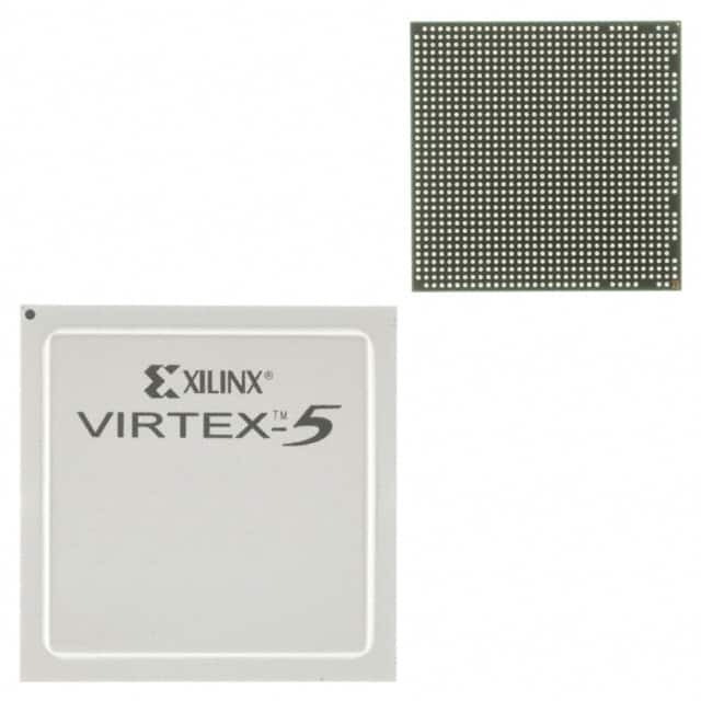
XC5VLX85-1FFG1153C
Product Overview
Category
XC5VLX85-1FFG1153C belongs to the category of Field Programmable Gate Arrays (FPGAs).
Use
This FPGA is designed for high-performance applications that require programmable logic solutions.
Characteristics
- High-performance FPGA with advanced features
- Offers flexibility and reconfigurability
- Suitable for complex digital designs
- Provides high-speed data processing capabilities
Package
XC5VLX85-1FFG1153C comes in a compact package, which ensures easy integration into electronic systems.
Essence
The essence of XC5VLX85-1FFG1153C lies in its ability to provide a customizable hardware solution for various applications.
Packaging/Quantity
This FPGA is typically packaged individually and is available in varying quantities depending on the customer's requirements.
Specifications
- Model: XC5VLX85-1FFG1153C
- Logic Cells: 84,960
- Number of DSP Slices: 352
- Maximum Frequency: 550 MHz
- Operating Voltage: 1.2V
- I/O Pins: 1,153
- Memory Size: 4,608 Kbits
- Package Type: Flip-Chip BGA
Detailed Pin Configuration
The detailed pin configuration of XC5VLX85-1FFG1153C can be found in the product datasheet provided by the manufacturer. It includes information about the specific functions and connections of each pin.
Functional Features
XC5VLX85-1FFG1153C offers several functional features that make it suitable for a wide range of applications:
- High-speed data processing capabilities
- Configurable logic cells for custom designs
- Integrated DSP slices for signal processing tasks
- Flexible I/O options for interfacing with external devices
- On-chip memory for data storage and retrieval
Advantages and Disadvantages
Advantages
- High-performance FPGA suitable for complex designs
- Flexibility and reconfigurability for customization
- Advanced features for signal processing tasks
- Wide range of I/O options for interfacing with external devices
Disadvantages
- Relatively high power consumption compared to other programmable logic devices
- Steeper learning curve for beginners due to the complexity of FPGA programming
Working Principles
XC5VLX85-1FFG1153C operates based on the principles of field-programmable gate arrays. It consists of configurable logic cells, interconnects, and various functional blocks that can be programmed to perform specific tasks. The FPGA is programmed using a hardware description language (HDL) such as VHDL or Verilog, which defines the desired functionality of the circuit. Once programmed, the FPGA can execute the specified operations.
Detailed Application Field Plans
XC5VLX85-1FFG1153C finds applications in various fields, including:
- Telecommunications: Used in high-speed data transmission systems and network infrastructure equipment.
- Aerospace and Defense: Employed in radar systems, avionics, and military communication devices.
- Industrial Automation: Utilized in control systems, robotics, and machine vision applications.
- Medical Electronics: Applied in medical imaging, patient monitoring, and diagnostic equipment.
- Automotive: Used in advanced driver assistance systems (ADAS), infotainment systems, and engine control units (ECUs).
Detailed and Complete Alternative Models
- XC5VLX50-1FFG676C: A lower-cost alternative with similar features but reduced logic cell count.
- XC5VLX110-1FFG1153C: A higher-capacity option with increased logic cells and I/O pins.
- XC5VLX330-1FFG1760C: A more powerful alternative with a larger number of logic cells and DSP slices.
These alternative models provide customers with options that cater to their specific requirements, allowing them to choose the most suitable FPGA for their applications.
Word count: 550 words
기술 솔루션에 XC5VLX85-1FFG1153C 적용과 관련된 10가지 일반적인 질문과 답변을 나열하세요.
Sure! Here are 10 common questions and answers related to the application of XC5VLX85-1FFG1153C in technical solutions:
Q1: What is XC5VLX85-1FFG1153C? A1: XC5VLX85-1FFG1153C is a field-programmable gate array (FPGA) manufactured by Xilinx. It is part of the Virtex-5 family and offers a range of features and capabilities for implementing complex digital designs.
Q2: What are the key specifications of XC5VLX85-1FFG1153C? A2: The key specifications include 85,000 logic cells, 1,153 available I/O pins, a maximum operating frequency of 550 MHz, and support for various communication protocols such as PCIe, Ethernet, and USB.
Q3: What are some typical applications of XC5VLX85-1FFG1153C? A3: XC5VLX85-1FFG1153C can be used in a wide range of applications including telecommunications, aerospace, defense, industrial automation, medical devices, and high-performance computing.
Q4: How can XC5VLX85-1FFG1153C be programmed? A4: XC5VLX85-1FFG1153C can be programmed using Xilinx's Vivado Design Suite or ISE Design Suite software tools. These tools allow designers to create and implement their digital designs on the FPGA.
Q5: What are the advantages of using XC5VLX85-1FFG1153C in technical solutions? A5: Some advantages include its high logic capacity, extensive I/O capabilities, support for various communication protocols, and the flexibility of being a programmable device that can be reconfigured as needed.
Q6: Can XC5VLX85-1FFG1153C be used in safety-critical applications? A6: Yes, XC5VLX85-1FFG1153C can be used in safety-critical applications. However, it is important to follow appropriate design and verification processes to ensure the reliability and integrity of the system.
Q7: What are the power requirements for XC5VLX85-1FFG1153C? A7: The power requirements depend on the specific implementation and configuration of the FPGA. It is recommended to refer to the datasheet and design guidelines provided by Xilinx for detailed power considerations.
Q8: Can XC5VLX85-1FFG1153C interface with other components or devices? A8: Yes, XC5VLX85-1FFG1153C can interface with other components or devices through its available I/O pins. It supports various communication protocols such as LVDS, DDR, SPI, I2C, and more.
Q9: Are there any limitations or constraints when using XC5VLX85-1FFG1153C? A9: Some limitations include the finite number of logic cells and I/O pins, limited resources for implementing complex designs, and potential power and thermal considerations depending on the application.
Q10: Where can I find additional resources and support for XC5VLX85-1FFG1153C? A10: Xilinx provides comprehensive documentation, application notes, reference designs, and technical support through their website. Additionally, online forums and communities dedicated to FPGA development can also be helpful sources of information.