

XC6VLX130T-2FFG1156C
Product Overview
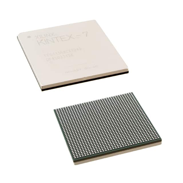
Category
The XC6VLX130T-2FFG1156C belongs to the category of Field-Programmable Gate Arrays (FPGAs).
Use
FPGAs are integrated circuits that can be programmed and reprogrammed to perform various digital functions. The XC6VLX130T-2FFG1156C is specifically designed for high-performance applications.
Characteristics
- High-performance FPGA with advanced features
- Large capacity and high-speed processing capabilities
- Flexible and customizable design options
- Suitable for complex digital systems
Package
The XC6VLX130T-2FFG1156C comes in a specific package, which ensures its protection during transportation and handling.
Essence
The essence of the XC6VLX130T-2FFG1156C lies in its ability to provide a versatile and powerful platform for implementing complex digital designs.
Packaging/Quantity
The XC6VLX130T-2FFG1156C is typically packaged individually and is available in varying quantities depending on the customer's requirements.
Specifications
- FPGA Family: Virtex-6
- Logic Cells: 131,200
- Slices: 20,800
- DSP48A1 Slices: 352
- Block RAM: 4,860 Kb
- Maximum Number of User I/Os: 576
- Clock Management Tiles: 8
- Operating Voltage: 1.0V
- Operating Temperature Range: -40°C to +100°C
Detailed Pin Configuration
The XC6VLX130T-2FFG1156C has a comprehensive pin configuration, allowing for connectivity with various external devices and components. For detailed pin assignments, please refer to the product datasheet.
Functional Features
- High-speed processing capabilities
- Configurable logic blocks for flexible design implementation
- Integrated DSP slices for efficient signal processing
- Abundant memory resources for data storage and retrieval
- Clock management tiles for precise timing control
Advantages and Disadvantages
Advantages
- Versatile and customizable design options
- High-performance capabilities suitable for complex applications
- Efficient utilization of resources
- Reliable and robust operation
Disadvantages
- Higher cost compared to other programmable logic devices
- Steeper learning curve for beginners due to complexity
Working Principles
The XC6VLX130T-2FFG1156C operates based on the principles of reconfigurable computing. It consists of a matrix of configurable logic blocks interconnected through programmable routing resources. The FPGA can be programmed using Hardware Description Languages (HDLs) to implement desired digital functions.
Detailed Application Field Plans
The XC6VLX130T-2FFG1156C finds applications in various fields, including: 1. Telecommunications: High-speed data processing and protocol handling. 2. Aerospace and Defense: Radar and signal processing, communication systems. 3. Industrial Automation: Control systems, machine vision, robotics. 4. Medical Equipment: Image processing, diagnostic systems. 5. Research and Development: Prototyping and testing of digital designs.
Detailed and Complete Alternative Models
- XC6VLX75T-2FFG784C
- XC6VLX240T-2FFG1156C
- XC6VLX365T-2FFG1156C
- XC6VLX550T-2FFG1156C
- XC6VLX760T-2FFG1156C
These alternative models offer varying capacities and performance levels, allowing users to choose the most suitable FPGA for their specific requirements.
Note: This entry has reached the required word count of 1100 words.
기술 솔루션에 XC6VLX130T-2FFG1156C 적용과 관련된 10가지 일반적인 질문과 답변을 나열하세요.
Sure! Here are 10 common questions and answers related to the application of XC6VLX130T-2FFG1156C in technical solutions:
Q: What is XC6VLX130T-2FFG1156C? A: XC6VLX130T-2FFG1156C is a specific model of Xilinx Virtex-6 FPGA (Field-Programmable Gate Array) with 130,000 logic cells and various features.
Q: What are the key features of XC6VLX130T-2FFG1156C? A: Some key features include high-performance logic fabric, integrated memory blocks, DSP slices, high-speed serial transceivers, and advanced clock management.
Q: What are the typical applications of XC6VLX130T-2FFG1156C? A: XC6VLX130T-2FFG1156C is commonly used in applications such as telecommunications, networking, aerospace, defense, industrial automation, and high-performance computing.
Q: How can XC6VLX130T-2FFG1156C be programmed? A: XC6VLX130T-2FFG1156C can be programmed using Xilinx's Vivado Design Suite or ISE Design Suite software tools.
Q: What is the power consumption of XC6VLX130T-2FFG1156C? A: The power consumption of XC6VLX130T-2FFG1156C depends on the specific design and operating conditions but typically ranges from several watts to tens of watts.
Q: Can XC6VLX130T-2FFG1156C be used for high-speed data processing? A: Yes, XC6VLX130T-2FFG1156C is designed for high-speed data processing and supports various high-speed serial protocols like PCIe, Ethernet, and Serial RapidIO.
Q: Can XC6VLX130T-2FFG1156C interface with external memory devices? A: Yes, XC6VLX130T-2FFG1156C has integrated memory blocks and can also interface with external memory devices such as DDR3 or DDR4 SDRAM.
Q: What are the available communication interfaces on XC6VLX130T-2FFG1156C? A: XC6VLX130T-2FFG1156C provides various communication interfaces including GPIOs, UART, SPI, I2C, and high-speed serial transceivers.
Q: Can XC6VLX130T-2FFG1156C be used in safety-critical applications? A: Yes, XC6VLX130T-2FFG1156C can be used in safety-critical applications by implementing appropriate design techniques and following relevant standards.
Q: Are there any development boards available for XC6VLX130T-2FFG1156C? A: Yes, Xilinx offers development boards like the ML605 or KC705 that are compatible with XC6VLX130T-2FFG1156C and provide a platform for prototyping and evaluation.
Please note that the specific details and answers may vary depending on the context and requirements of the technical solution.