

XC6VLX240T-1FFG1156C
Product Overview
Category
The XC6VLX240T-1FFG1156C belongs to the category of Field Programmable Gate Arrays (FPGAs).
Use
FPGAs are integrated circuits that can be programmed and reprogrammed to perform various digital functions. They are widely used in industries such as telecommunications, automotive, aerospace, and consumer electronics.
Characteristics
The XC6VLX240T-1FFG1156C is known for its high performance and versatility. It offers a large number of logic cells, abundant memory resources, and flexible I/O options. These characteristics make it suitable for complex digital designs and applications that require high-speed processing.
Package
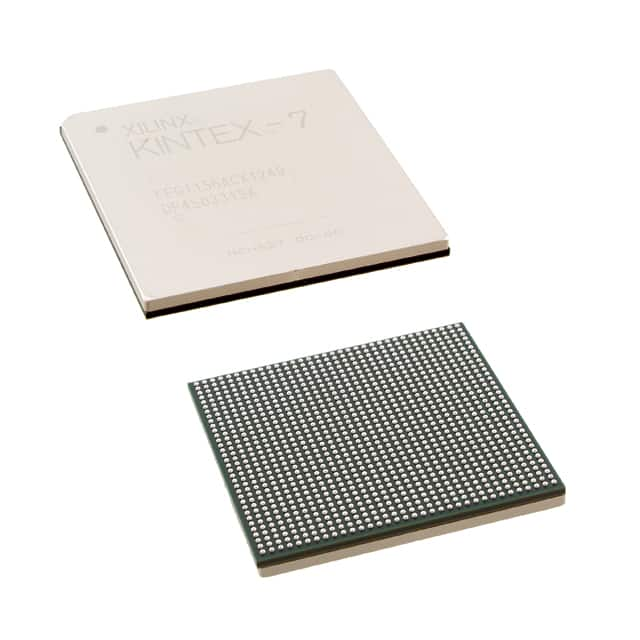
The XC6VLX240T-1FFG1156C is available in a Flip-Chip Fine-Pitch Ball Grid Array (FFG1156) package. This package provides excellent thermal performance and allows for easy integration onto printed circuit boards.
Essence
The essence of the XC6VLX240T-1FFG1156C lies in its ability to provide a customizable hardware platform that can be tailored to specific application requirements. Its programmability allows designers to implement complex algorithms and functions in hardware, resulting in improved performance and efficiency.
Packaging/Quantity
The XC6VLX240T-1FFG1156C is typically sold in trays or reels, depending on the manufacturer's packaging standards. The quantity per package may vary, but it is commonly available in quantities of 10 or more.
Specifications
- Logic Cells: 240,000
- Block RAM: 4,860 Kb
- DSP Slices: 720
- Maximum Frequency: 550 MHz
- I/O Pins: 1,156
- Operating Voltage: 1.0V - 1.2V
- Operating Temperature: -40°C to 100°C
Detailed Pin Configuration
The XC6VLX240T-1FFG1156C has a complex pin configuration with multiple I/O banks, power supply pins, and configuration pins. For detailed information on the pin configuration, please refer to the manufacturer's datasheet.
Functional Features
- High-performance FPGA with abundant logic resources
- Flexible I/O options for interfacing with external devices
- Configurable memory blocks for efficient data storage
- Dedicated DSP slices for implementing complex mathematical operations
- Built-in clock management resources for precise timing control
- Support for various communication protocols and standards
Advantages and Disadvantages
Advantages
- High performance and versatility
- Customizable hardware platform
- Efficient implementation of complex algorithms
- Wide range of application possibilities
- Easy integration onto printed circuit boards
Disadvantages
- Steep learning curve for beginners
- Higher cost compared to other programmable logic devices
- Limited availability of alternative models with similar specifications
Working Principles
FPGAs like the XC6VLX240T-1FFG1156C consist of an array of configurable logic blocks interconnected through programmable routing resources. The device is programmed using a Hardware Description Language (HDL) such as VHDL or Verilog. The HDL code describes the desired functionality, which is then synthesized and implemented on the FPGA. During operation, the FPGA executes the programmed logic, performing the desired functions in real-time.
Detailed Application Field Plans
The XC6VLX240T-1FFG1156C finds applications in various fields, including:
- Telecommunications: Used in base stations, routers, and network switches for high-speed data processing and protocol handling.
- Automotive: Employed in advanced driver-assistance systems (ADAS), infotainment systems, and engine control units (ECUs) for real-time data processing and control.
- Aerospace: Utilized in satellite communication systems, avionics, and radar systems for high-performance signal processing and control.
- Consumer Electronics: Integrated into high-definition televisions, gaming consoles, and multimedia devices for video and audio processing.
Detailed and Complete Alternative Models
While the XC6VLX240T-1FFG1156C offers a unique combination of features and specifications, there are alternative models available from other FPGA manufacturers. Some notable alternatives include:
- Intel Cyclone V GX: Offers similar performance and flexibility with a different architecture.
- Lattice ECP5: Provides a lower-cost option with comparable logic resources and I/O capabilities.
- Microchip PolarFire: Focuses on low-power applications while maintaining high performance and security features.
These alternative models can be considered based on specific project requirements and cost considerations.
In conclusion, the XC6VLX240T-1FFG1156C is a high-performance FPGA that offers versatility and customization options. Its advanced features make it suitable for a wide range of applications in various industries.
기술 솔루션에 XC6VLX240T-1FFG1156C 적용과 관련된 10가지 일반적인 질문과 답변을 나열하세요.
Sure! Here are 10 common questions and answers related to the application of XC6VLX240T-1FFG1156C in technical solutions:
Q1: What is XC6VLX240T-1FFG1156C? A1: XC6VLX240T-1FFG1156C is a field-programmable gate array (FPGA) manufactured by Xilinx. It is part of the Virtex-6 family and offers high-performance capabilities for various applications.
Q2: What are the key features of XC6VLX240T-1FFG1156C? A2: Some key features of XC6VLX240T-1FFG1156C include a large number of logic cells, high-speed serial transceivers, embedded memory blocks, DSP slices, and support for various I/O standards.
Q3: What are the typical applications of XC6VLX240T-1FFG1156C? A3: XC6VLX240T-1FFG1156C can be used in a wide range of applications such as telecommunications, networking, video processing, aerospace, defense, industrial automation, and scientific research.
Q4: How does XC6VLX240T-1FFG1156C compare to other FPGAs? A4: XC6VLX240T-1FFG1156C offers a good balance between performance, capacity, and power consumption. It provides a higher logic density compared to some lower-end FPGAs while being more cost-effective than higher-end FPGAs.
Q5: Can XC6VLX240T-1FFG1156C be used for high-speed data processing? A5: Yes, XC6VLX240T-1FFG1156C supports high-speed serial transceivers, which make it suitable for applications requiring high-speed data processing, such as high-frequency trading or real-time video processing.
Q6: What development tools are available for XC6VLX240T-1FFG1156C? A6: Xilinx provides a suite of development tools, including Vivado Design Suite, ISE Design Suite, and various IP cores, to facilitate the design, implementation, and verification of FPGA designs using XC6VLX240T-1FFG1156C.
Q7: Can XC6VLX240T-1FFG1156C be used in safety-critical applications? A7: Yes, XC6VLX240T-1FFG1156C can be used in safety-critical applications. However, additional measures, such as redundancy and fault-tolerant design techniques, may need to be implemented to ensure the required level of reliability.
Q8: How can I interface XC6VLX240T-1FFG1156C with other components or systems? A8: XC6VLX240T-1FFG1156C supports various I/O standards, such as LVCMOS, LVDS, and differential signaling, which allow for easy interfacing with other components or systems. Additionally, it provides configurable I/O banks and programmable I/O voltage levels.
Q9: Can XC6VLX240T-1FFG1156C be reprogrammed after deployment? A9: Yes, XC6VLX240T-1FFG1156C is a field-programmable device, meaning that it can be reprogrammed even after it has been deployed in a system. This flexibility allows for iterative design improvements and updates.
Q10: Are there any known limitations or considerations when using XC6VLX240T-1FFG1156C? A10: Some considerations include power consumption, thermal management, and the need for proper design techniques to optimize performance and resource utilization. Additionally, it is important to consider the specific requirements of your application and consult the device datasheet and user guides for detailed information.
Please note that these answers are general and may vary depending on the specific requirements and context of your technical solution.