

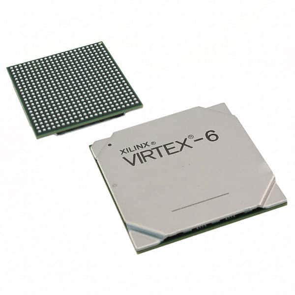
XC6VLX365T-2FF1759I
Product Overview
Category
The XC6VLX365T-2FF1759I belongs to the category of Field Programmable Gate Arrays (FPGAs).
Use
FPGAs are integrated circuits that can be programmed after manufacturing, allowing for flexible and customizable digital logic designs. The XC6VLX365T-2FF1759I is specifically designed for high-performance applications.
Characteristics
- High-performance FPGA with advanced features
- Large capacity and high-speed processing capabilities
- Flexible and reprogrammable design
- Suitable for complex digital logic designs
- Ideal for applications requiring high-speed data processing and real-time performance
Package
The XC6VLX365T-2FF1759I comes in a compact and durable package, ensuring easy handling and protection during transportation and installation.
Essence
The essence of the XC6VLX365T-2FF1759I lies in its ability to provide a versatile and powerful platform for implementing complex digital logic designs.
Packaging/Quantity
The XC6VLX365T-2FF1759I is typically packaged individually and is available in various quantities depending on the customer's requirements.
Specifications
- FPGA Family: Virtex-6
- Logic Cells: 365,000
- Slices: 57,600
- DSP48A1 Slices: 760
- Block RAM: 4,860 Kb
- Maximum Number of User I/Os: 800
- Clock Management Tiles: 16
- Maximum Frequency: 550 MHz
- Operating Voltage: 1.0V
Detailed Pin Configuration
The XC6VLX365T-2FF1759I has a comprehensive pin configuration, enabling connectivity with external devices and components. For detailed pin assignments, please refer to the manufacturer's datasheet.
Functional Features
- High-performance processing capabilities
- Flexible and reprogrammable design
- Advanced clock management features
- Integrated DSP slices for efficient signal processing
- Large capacity for complex designs
- Support for various communication protocols
- On-chip memory resources for data storage and retrieval
Advantages and Disadvantages
Advantages
- High-speed processing capabilities
- Flexibility in design and customization
- Efficient utilization of system resources
- Support for various communication protocols
- On-chip memory resources for data storage
Disadvantages
- Higher power consumption compared to other alternatives
- Steeper learning curve for beginners
- Relatively higher cost compared to simpler programmable logic devices
Working Principles
The XC6VLX365T-2FF1759I operates based on the principles of field-programmable gate arrays. It consists of a large number of configurable logic blocks interconnected through programmable routing resources. The device can be programmed using Hardware Description Languages (HDLs) such as VHDL or Verilog, allowing users to define the desired digital logic functionality. Once programmed, the FPGA executes the defined logic operations, providing high-speed processing capabilities.
Detailed Application Field Plans
The XC6VLX365T-2FF1759I finds applications in various fields that require high-performance digital logic processing. Some potential application areas include:
- Telecommunications: Implementing high-speed data processing and protocol conversion.
- Aerospace and Defense: Real-time signal processing, radar systems, and secure communications.
- Industrial Automation: Control systems, motor control, and data acquisition.
- Medical Imaging: Image processing and analysis for medical diagnostics.
- Scientific Research: Data analysis, simulation, and modeling.
Detailed and Complete Alternative Models
- XC6VLX240T-2FFG1156C
- XC6VLX550T-2FFG1759C
- XC6VLX130T-2FFG1156I
- XC6VLX75T-2FFG784I
These alternative models offer varying capacities and features, allowing users to choose the most suitable FPGA for their specific requirements.
Note: The content provided above is a general overview of the XC6VLX365T-2FF1759I. For detailed technical specifications and further information, please refer to the manufacturer's documentation.
기술 솔루션에 XC6VLX365T-2FF1759I 적용과 관련된 10가지 일반적인 질문과 답변을 나열하세요.
Sure! Here are 10 common questions and answers related to the application of XC6VLX365T-2FF1759I in technical solutions:
Question: What is the XC6VLX365T-2FF1759I?
Answer: The XC6VLX365T-2FF1759I is a field-programmable gate array (FPGA) from Xilinx, designed for high-performance applications.Question: What are the key features of the XC6VLX365T-2FF1759I?
Answer: Some key features include a large number of logic cells, high-speed serial transceivers, embedded memory blocks, and advanced DSP capabilities.Question: In what types of technical solutions can the XC6VLX365T-2FF1759I be used?
Answer: It can be used in a wide range of applications such as telecommunications, aerospace, defense, industrial automation, and high-performance computing.Question: What is the maximum operating frequency of the XC6VLX365T-2FF1759I?
Answer: The maximum operating frequency depends on the specific design and implementation, but it can reach up to several hundred megahertz.Question: Can the XC6VLX365T-2FF1759I support multiple communication protocols?
Answer: Yes, it has built-in high-speed serial transceivers that can support various communication protocols like PCIe, Ethernet, SATA, and more.Question: How much logic capacity does the XC6VLX365T-2FF1759I offer?
Answer: It provides around 365,000 logic cells, which can be used to implement complex digital designs.Question: Does the XC6VLX365T-2FF1759I have any built-in memory?
Answer: Yes, it has embedded memory blocks that can be used for storing data or implementing memory-intensive algorithms.Question: Can the XC6VLX365T-2FF1759I perform digital signal processing (DSP) operations?
Answer: Yes, it has dedicated DSP slices that can accelerate various mathematical operations commonly used in signal processing applications.Question: What development tools are available for programming the XC6VLX365T-2FF1759I?
Answer: Xilinx provides a suite of development tools, including Vivado Design Suite, which allows designers to program and configure the FPGA.Question: Are there any specific design considerations when using the XC6VLX365T-2FF1759I?
Answer: Yes, designers need to consider factors like power consumption, thermal management, and signal integrity when integrating the FPGA into their technical solutions.
Please note that the answers provided here are general and may vary depending on the specific requirements and context of each application.