

XC7K325T-L2FFG900E
Product Overview
Category
XC7K325T-L2FFG900E belongs to the category of Field-Programmable Gate Arrays (FPGAs).
Use
This FPGA is designed for various applications that require high-performance processing, such as telecommunications, data centers, industrial automation, and scientific research.
Characteristics
- High-speed processing capabilities
- Configurable logic blocks
- On-chip memory resources
- Flexible I/O interfaces
- Low power consumption
Package
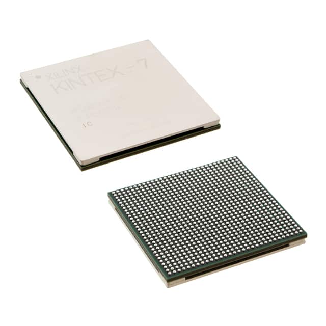
XC7K325T-L2FFG900E comes in a compact package suitable for integration into electronic systems. The package ensures efficient heat dissipation and protection against external factors.
Essence
The essence of XC7K325T-L2FFG900E lies in its ability to provide reconfigurable hardware that can be customized to meet specific application requirements.
Packaging/Quantity
Each package of XC7K325T-L2FFG900E contains one FPGA unit.
Specifications
- Logic Cells: 325,000
- DSP Slices: 1,920
- Block RAM: 36 Mb
- Maximum Frequency: 550 MHz
- I/O Pins: 900
- Operating Voltage: 1.0V - 1.2V
- Operating Temperature Range: -40°C to 100°C
Detailed Pin Configuration
For a detailed pin configuration diagram of XC7K325T-L2FFG900E, please refer to the manufacturer's datasheet or documentation.
Functional Features
XC7K325T-L2FFG900E offers the following functional features:
- High-speed data processing
- Parallel computing capabilities
- Support for various communication protocols
- Efficient resource utilization
- Dynamic reconfiguration
Advantages and Disadvantages
Advantages
- Versatile and adaptable to different applications
- High-performance processing capabilities
- Low power consumption
- Flexible I/O interfaces
Disadvantages
- Relatively high cost compared to other FPGA options
- Steeper learning curve for programming and configuration
Working Principles
XC7K325T-L2FFG900E operates based on the principles of reconfigurable hardware. It consists of configurable logic blocks, memory resources, and I/O interfaces that can be programmed to perform specific tasks. The FPGA's internal architecture allows for parallel processing and efficient utilization of available resources.
Detailed Application Field Plans
XC7K325T-L2FFG900E finds applications in various fields, including:
- Telecommunications: Used in network routers, switches, and base stations for high-speed data processing.
- Data Centers: Employed for accelerating data analytics, virtualization, and cloud computing tasks.
- Industrial Automation: Utilized in control systems, robotics, and machine vision applications.
- Scientific Research: Applied in scientific simulations, signal processing, and data acquisition systems.
Alternative Models
For alternative models with similar capabilities, consider the following options:
- XC7K160T-L2FFG900E
- XC7K410T-L2FFG900E
- XC7K480T-L2FFG900E
These models offer varying levels of logic capacity, I/O pins, and performance characteristics, allowing users to choose the most suitable option for their specific requirements.
In conclusion, XC7K325T-L2FFG900E is a high-performance FPGA that offers versatile functionality, making it suitable for a wide range of applications. Its configurable nature, along with its advanced features, provides flexibility and efficiency in system design and implementation.
Word Count: 520
기술 솔루션에 XC7K325T-L2FFG900E 적용과 관련된 10가지 일반적인 질문과 답변을 나열하세요.
Sure! Here are 10 common questions and answers related to the application of XC7K325T-L2FFG900E in technical solutions:
Question: What is the XC7K325T-L2FFG900E?
Answer: The XC7K325T-L2FFG900E is a specific model of Xilinx's Kintex-7 FPGA family, which offers high-performance programmable logic capabilities.Question: What are the key features of the XC7K325T-L2FFG900E?
Answer: Some key features include a large number of programmable logic cells, high-speed serial transceivers, integrated memory blocks, and advanced DSP capabilities.Question: In what technical solutions can the XC7K325T-L2FFG900E be used?
Answer: The XC7K325T-L2FFG900E can be used in various applications such as wireless communication systems, video processing, industrial automation, aerospace, and defense.Question: What is the maximum operating frequency of the XC7K325T-L2FFG900E?
Answer: The maximum operating frequency depends on the design and implementation, but it can reach up to several hundred megahertz or even gigahertz.Question: How much programmable logic capacity does the XC7K325T-L2FFG900E offer?
Answer: The XC7K325T-L2FFG900E provides around 325,000 logic cells, which can be used for implementing complex digital designs.Question: Can the XC7K325T-L2FFG900E interface with external devices?
Answer: Yes, the XC7K325T-L2FFG900E has various I/O standards and interfaces, including LVCMOS, LVDS, PCI Express, Ethernet, and more, allowing it to communicate with external devices.Question: What development tools are available for programming the XC7K325T-L2FFG900E?
Answer: Xilinx provides Vivado Design Suite, which includes a comprehensive set of tools for designing, implementing, and debugging FPGA designs.Question: Can the XC7K325T-L2FFG900E be reprogrammed after deployment?
Answer: Yes, FPGAs like the XC7K325T-L2FFG900E can be reprogrammed multiple times, making them flexible for future updates or changes in functionality.Question: Are there any power requirements for the XC7K325T-L2FFG900E?
Answer: Yes, the XC7K325T-L2FFG900E requires a specific power supply voltage and current, which should be provided according to the manufacturer's specifications.Question: Where can I find more information about the XC7K325T-L2FFG900E?
Answer: You can refer to the official documentation and datasheets provided by Xilinx, as well as online forums and communities dedicated to FPGA development.