

XC7K70T-2FBG484I
Product Overview
Category
The XC7K70T-2FBG484I belongs to the category of Field-Programmable Gate Arrays (FPGAs).
Use
FPGAs are integrated circuits that can be programmed and reprogrammed to perform various digital functions. The XC7K70T-2FBG484I is specifically designed for high-performance applications that require complex logic functions.
Characteristics
- High-performance FPGA with advanced features
- Programmable and reconfigurable
- Offers a large number of logic cells and I/O pins
- Supports high-speed data processing
- Provides flexibility in designing custom digital circuits
Package
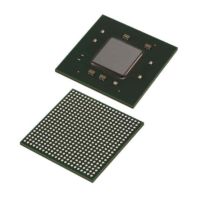
The XC7K70T-2FBG484I comes in a FBG484 package, which refers to a Fine-Pitch Ball Grid Array with 484 balls. This package provides a compact form factor and facilitates easy integration into electronic systems.
Essence
The essence of the XC7K70T-2FBG484I lies in its ability to provide a versatile platform for implementing complex digital designs. It offers a wide range of features and capabilities that enable designers to create customized solutions for various applications.
Packaging/Quantity
The XC7K70T-2FBG484I is typically sold individually or in small quantities, depending on the supplier. The packaging ensures the safe transportation and handling of the FPGA.
Specifications
- Logic Cells: 68,200
- Flip-Flops: 34,100
- Block RAM: 2,700 Kbits
- DSP Slices: 740
- Maximum Frequency: 600 MHz
- I/O Pins: 400
- Voltage Range: 1.0V - 1.2V
Detailed Pin Configuration
The XC7K70T-2FBG484I has a total of 400 I/O pins, which are configurable based on the specific requirements of the design. The pin configuration can be customized using FPGA design software, allowing designers to connect the FPGA to external devices and circuits as needed.
Functional Features
- High-performance processing capabilities
- Configurable logic cells for implementing complex functions
- Dedicated DSP slices for efficient digital signal processing
- Flexible I/O options for interfacing with external devices
- On-chip memory blocks for data storage and retrieval
- Support for various communication protocols and standards
Advantages and Disadvantages
Advantages
- Versatile and flexible platform for digital circuit design
- High-performance processing capabilities
- Reconfigurable nature allows for iterative development and testing
- Large number of logic cells and I/O pins provide ample resources for complex designs
- Support for various communication protocols and standards enhances compatibility
Disadvantages
- Steep learning curve for beginners due to the complexity of FPGA programming
- Higher cost compared to other programmable logic devices
- Power consumption can be relatively high, especially for resource-intensive applications
Working Principles
The XC7K70T-2FBG484I operates based on the principles of reconfigurable computing. It consists of an array of configurable logic cells interconnected through programmable routing resources. These logic cells can be programmed to implement desired digital functions by configuring their internal connections and behavior.
The FPGA is programmed using Hardware Description Languages (HDLs) such as VHDL or Verilog. The HDL code describes the desired functionality of the digital circuit, which is then synthesized and implemented on the FPGA. Once programmed, the FPGA can perform the specified functions and can be reprogrammed as needed.
Detailed Application Field Plans
The XC7K70T-2FBG484I finds application in various fields that require high-performance digital processing. Some potential application areas include:
- Telecommunications: FPGA-based solutions are used in communication systems for signal processing, protocol implementation, and network optimization.
- Aerospace and Defense: FPGAs are utilized in radar systems, avionics, and military-grade communication equipment due to their high-speed processing capabilities and reconfigurability.
- Industrial Automation: FPGAs play a crucial role in industrial control systems, robotics, and machine vision applications, enabling real-time data processing and control.
- Medical Devices: FPGAs are employed in medical imaging systems, patient monitoring devices, and diagnostic equipment for efficient data processing and analysis.
- Research and Development: FPGAs serve as a valuable tool for prototyping and testing new digital designs, allowing researchers and engineers to quickly iterate and refine their concepts.
Detailed and Complete Alternative Models
- XC7K70T-1FBG484I: Similar to the XC7K70T-2FBG484I, but with a lower maximum frequency of 550 MHz.
- XC7K70T-3FBG484I: Similar to the XC7K70T-2FBG484I,
기술 솔루션에 XC7K70T-2FBG484I 적용과 관련된 10가지 일반적인 질문과 답변을 나열하세요.
Sure! Here are 10 common questions and answers related to the application of XC7K70T-2FBG484I in technical solutions:
Q: What is XC7K70T-2FBG484I? A: XC7K70T-2FBG484I is a specific model of Xilinx's Kintex-7 FPGA (Field-Programmable Gate Array) family, designed for high-performance applications.
Q: What are the key features of XC7K70T-2FBG484I? A: Some key features include a high logic density, advanced DSP capabilities, high-speed serial connectivity, and support for various I/O standards.
Q: What are the typical applications of XC7K70T-2FBG484I? A: XC7K70T-2FBG484I is commonly used in applications such as wireless communication systems, video processing, industrial automation, aerospace, and defense.
Q: How can XC7K70T-2FBG484I be programmed? A: XC7K70T-2FBG484I can be programmed using Xilinx's Vivado Design Suite, which provides a comprehensive development environment for FPGA designs.
Q: What is the power consumption of XC7K70T-2FBG484I? A: The power consumption of XC7K70T-2FBG484I depends on the specific design and operating conditions. It is recommended to refer to the datasheet for detailed power specifications.
Q: Can XC7K70T-2FBG484I be used in safety-critical applications? A: Yes, XC7K70T-2FBG484I can be used in safety-critical applications. However, it is important to follow appropriate design and verification practices to ensure the required level of safety.
Q: What are the available interfaces on XC7K70T-2FBG484I? A: XC7K70T-2FBG484I provides various interfaces, including high-speed transceivers, DDR3 memory controllers, PCIe, Ethernet, USB, and general-purpose I/Os.
Q: Can XC7K70T-2FBG484I be used for real-time signal processing? A: Yes, XC7K70T-2FBG484I is well-suited for real-time signal processing applications due to its high-performance capabilities and support for advanced DSP functions.
Q: Is there any specific development board available for XC7K70T-2FBG484I? A: Xilinx offers several development boards that are compatible with XC7K70T-2FBG484I, such as the Kintex-7 KC705 Evaluation Kit, which provides a platform for prototyping and testing designs.
Q: Are there any application notes or reference designs available for XC7K70T-2FBG484I? A: Yes, Xilinx provides a wide range of application notes, reference designs, and documentation to assist users in implementing XC7K70T-2FBG484I in their technical solutions. These resources can be found on the Xilinx website.