

XC7VX980T-1FFG1928I
Product Overview
Category
The XC7VX980T-1FFG1928I belongs to the category of Field-Programmable Gate Arrays (FPGAs).
Use
FPGAs are integrated circuits that can be programmed and reprogrammed to perform various digital functions. The XC7VX980T-1FFG1928I is specifically designed for high-performance applications that require complex logic and processing capabilities.
Characteristics
- High-performance FPGA with advanced features
- Large capacity and high-speed processing capabilities
- Flexible and reconfigurable design
- Suitable for demanding applications in industries such as telecommunications, aerospace, and defense
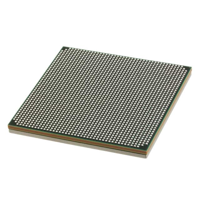
Package
The XC7VX980T-1FFG1928I comes in a specific package format, which ensures its physical protection and facilitates its integration into electronic systems.
Essence
The essence of the XC7VX980T-1FFG1928I lies in its ability to provide a customizable hardware platform that can be tailored to meet specific application requirements. It offers a balance between performance, flexibility, and power consumption.
Packaging/Quantity
The XC7VX980T-1FFG1928I is typically packaged individually and is available in varying quantities depending on the manufacturer or distributor.
Specifications
- Logic Cells: 980,000
- DSP Slices: 3,600
- Block RAM: 54 Mb
- Maximum I/O Pins: 1,928
- Operating Voltage: 1.0V
- Operating Temperature Range: -40°C to +100°C
- Package Type: Flip-Chip Fine-Pitch BGA (FFG)
- Package Pins: 1,928
Detailed Pin Configuration
The XC7VX980T-1FFG1928I has a comprehensive pin configuration that allows for connectivity with external devices and components. The detailed pin configuration can be found in the product datasheet provided by the manufacturer.
Functional Features
- High-performance processing capabilities
- Configurable logic blocks for custom circuit implementation
- Dedicated digital signal processing (DSP) slices for efficient mathematical operations
- Integrated memory blocks for data storage and retrieval
- Flexible I/O interfaces for communication with external devices
- Clock management resources for precise timing control
Advantages and Disadvantages
Advantages
- High processing power and performance
- Flexibility to adapt to changing requirements
- Reconfigurability allows for iterative development and testing
- Suitable for complex applications requiring real-time processing
- Availability of comprehensive development tools and support
Disadvantages
- Higher cost compared to other programmable logic devices
- Steeper learning curve for programming and design
- Power consumption may be higher compared to dedicated application-specific integrated circuits (ASICs)
- Limited availability of alternative models with similar specifications
Working Principles
The XC7VX980T-1FFG1928I operates based on the principles of reconfigurable computing. It consists of an array of configurable logic blocks interconnected through programmable routing resources. These logic blocks can be programmed to implement various digital functions, allowing for the creation of custom hardware designs.
The FPGA is configured by loading a bitstream into its internal memory, which defines the desired functionality. This configuration can be modified as needed, enabling the FPGA to adapt to different tasks or even perform multiple functions within a single device.
Detailed Application Field Plans
The XC7VX980T-1FFG1928I finds applications in various industries where high-performance and flexible processing capabilities are required. Some specific application field plans include:
- Telecommunications: Used in base stations, routers, and network switches to handle high-speed data processing and protocol conversion.
- Aerospace and Defense: Employed in radar systems, avionics, and satellite communication for real-time data processing and signal analysis.
- Industrial Automation: Utilized in control systems, robotics, and machine vision applications to enable high-speed data acquisition and processing.
- Scientific Research: Applied in scientific instruments, data acquisition systems, and simulation platforms for complex computational tasks.
Detailed and Complete Alternative Models
While the XC7VX980T-1FFG1928I offers a unique combination of features and specifications, there are alternative models available from other FPGA manufacturers. Some notable alternatives include:
- Intel Stratix 10 GX: Offers similar high-performance capabilities with a focus on power efficiency.
- Lattice ECP5: Provides a cost-effective solution with lower power consumption for certain applications.
- Microsemi SmartFusion2: Combines FPGA fabric with integrated ARM Cortex-M3 processor for embedded system designs.
These alternative models should be evaluated based on specific project requirements and constraints to determine the most suitable option.
In conclusion, the XC7VX980T-1FFG1928I is a high-performance
기술 솔루션에 XC7VX980T-1FFG1928I 적용과 관련된 10가지 일반적인 질문과 답변을 나열하세요.
Sure! Here are 10 common questions and answers related to the application of XC7VX980T-1FFG1928I in technical solutions:
Q1: What is XC7VX980T-1FFG1928I? A1: XC7VX980T-1FFG1928I is a high-performance field-programmable gate array (FPGA) manufactured by Xilinx.
Q2: What are the key features of XC7VX980T-1FFG1928I? A2: Some key features include a large number of logic cells, high-speed transceivers, embedded memory blocks, and advanced DSP capabilities.
Q3: What are the typical applications of XC7VX980T-1FFG1928I? A3: XC7VX980T-1FFG1928I is commonly used in applications such as telecommunications, aerospace, defense, video processing, and high-performance computing.
Q4: How can XC7VX980T-1FFG1928I be programmed? A4: XC7VX980T-1FFG1928I can be programmed using Xilinx's Vivado Design Suite, which provides a comprehensive development environment for FPGA designs.
Q5: What is the maximum operating frequency of XC7VX980T-1FFG1928I? A5: The maximum operating frequency of XC7VX980T-1FFG1928I depends on the specific design and implementation, but it can reach several hundred megahertz or even gigahertz.
Q6: Can XC7VX980T-1FFG1928I interface with other components or devices? A6: Yes, XC7VX980T-1FFG1928I supports various interfaces such as PCIe, Ethernet, USB, DDR3/DDR4 memory, and many more.
Q7: What are the power requirements for XC7VX980T-1FFG1928I? A7: The power requirements for XC7VX980T-1FFG1928I depend on the specific design and implementation. It typically requires multiple power supply rails with different voltage levels.
Q8: Can XC7VX980T-1FFG1928I be used in safety-critical applications? A8: Yes, XC7VX980T-1FFG1928I can be used in safety-critical applications. However, additional measures may need to be taken to ensure functional safety and reliability.
Q9: Are there any development boards or evaluation kits available for XC7VX980T-1FFG1928I? A9: Yes, Xilinx offers development boards and evaluation kits specifically designed for XC7VX980T-1FFG1928I, which provide a convenient platform for prototyping and testing.
Q10: Where can I find technical documentation and support for XC7VX980T-1FFG1928I? A10: Technical documentation, datasheets, application notes, and support resources for XC7VX980T-1FFG1928I can be found on Xilinx's official website or through their customer support channels.
Please note that the answers provided here are general and may vary depending on the specific requirements and use cases of XC7VX980T-1FFG1928I in different technical solutions.