

XCF16PFSG48C
Product Overview
Category: Integrated Circuit (IC)
Use: XCF16PFSG48C is a programmable logic device (PLD) used for digital circuit design and implementation. It offers high flexibility and customization options, making it suitable for various applications.
Characteristics: - Programmable: XCF16PFSG48C can be programmed to perform specific functions based on user requirements. - High-speed operation: It operates at high clock frequencies, enabling efficient data processing. - Low power consumption: The device is designed to minimize power consumption, making it energy-efficient. - Compact package: XCF16PFSG48C comes in a small form factor, allowing for space-saving integration into electronic systems. - Reliable performance: It offers reliable and stable operation, ensuring consistent functionality.
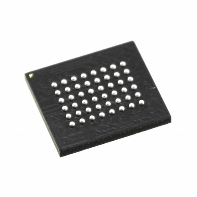
Package and Quantity: XCF16PFSG48C is available in a 48-pin small-grid array (SGA) package. Each package contains one unit of the device.
Essence: XCF16PFSG48C serves as a versatile building block for digital circuitry, providing designers with the ability to create custom logic functions tailored to their specific needs.
Packaging/Quantity: The XCF16PFSG48C is supplied in a protective anti-static packaging to prevent damage during transportation and storage. Each package contains one unit of the device.
Specifications
- Logic Cells: 16,000
- Maximum Operating Frequency: 200 MHz
- Input/Output Pins: 48
- Supply Voltage: 3.3V
- Operating Temperature Range: -40°C to +85°C
- Programming Method: In-system programmable (ISP)
- Configuration Memory: Non-volatile Flash memory
- Package Type: Small Grid Array (SGA)
- Package Dimensions: 7mm x 7mm
Detailed Pin Configuration
The XCF16PFSG48C has a total of 48 pins, each serving a specific purpose in the device's operation. The pin configuration is as follows:
(Pin Number - Pin Name - Description) 1 - VCCIO - I/O Power Supply 2 - GND - Ground 3 - VCCINT - Internal Power Supply 4 - DIN - Data Input 5 - DOUT - Data Output 6 - CS - Chip Select 7 - WE - Write Enable 8 - OE - Output Enable 9 - CLK - Clock Input 10-47 - I/O Pins - General-purpose Input/Output Pins 48 - NC - No Connection
Functional Features
- Programmability: XCF16PFSG48C can be programmed to implement various logic functions, allowing for customization and adaptability.
- High-Speed Operation: The device operates at high clock frequencies, enabling rapid data processing and efficient system performance.
- Flexible I/O Configuration: The I/O pins can be configured as inputs or outputs, providing versatility in interfacing with external devices.
- Non-volatile Configuration Memory: The device utilizes non-volatile Flash memory to store its configuration, ensuring that the programmed logic remains intact even after power cycles.
- JTAG Boundary Scan: XCF16PFSG48C supports Joint Test Action Group (JTAG) boundary scan, facilitating testing and debugging during the development process.
Advantages and Disadvantages
Advantages: - High flexibility and customization options - Compact form factor for space-saving integration - Reliable and stable performance - Low power consumption
Disadvantages: - Limited number of logic cells compared to higher-end PLDs - Relatively higher cost compared to simpler logic devices
Working Principles
XCF16PFSG48C operates based on the principles of programmable logic. It consists of a matrix of configurable logic blocks (CLBs) interconnected through programmable interconnects. The device's behavior is determined by the configuration data stored in its non-volatile memory. During operation, the input signals are processed through the configured logic functions, and the output signals are generated accordingly.
Detailed Application Field Plans
XCF16PFSG48C finds applications in various fields, including but not limited to: - Industrial automation - Communication systems - Consumer electronics - Automotive electronics - Medical devices - Aerospace and defense
The device's flexibility and programmability make it suitable for diverse applications that require custom logic implementation.
Detailed and Complete Alternative Models
- XCF32PFSG48C: Similar to XCF16PFSG48C but with double the number of logic cells.
- XCF8PFSG48C: A lower-capacity variant with 8,000 logic cells.
- XCF16PFSG64C: Similar to XCF16PFSG48C but with additional I/O pins.
These alternative models offer different capacity and pin configurations, allowing users to choose the most suitable option based on their specific requirements.
기술 솔루션에 XCF16PFSG48C 적용과 관련된 10가지 일반적인 질문과 답변을 나열하세요.
Sure! Here are 10 common questions and answers related to the application of XCF16PFSG48C in technical solutions:
Q: What is XCF16PFSG48C? A: XCF16PFSG48C is a specific model of a field-programmable gate array (FPGA) manufactured by Xilinx.
Q: What are the key features of XCF16PFSG48C? A: XCF16PFSG48C offers 16,000 logic cells, 48 I/O pins, and a non-volatile configuration memory.
Q: What is the typical power consumption of XCF16PFSG48C? A: The power consumption of XCF16PFSG48C varies depending on the design and usage, but it typically ranges from 100mW to 500mW.
Q: Can XCF16PFSG48C be used for high-speed applications? A: Yes, XCF16PFSG48C can be used for high-speed applications as it supports clock frequencies up to several hundred megahertz.
Q: How can XCF16PFSG48C be programmed? A: XCF16PFSG48C can be programmed using Xilinx's Vivado Design Suite or other compatible programming tools.
Q: Is XCF16PFSG48C suitable for industrial applications? A: Yes, XCF16PFSG48C is suitable for industrial applications due to its robustness, reliability, and extended temperature range support.
Q: Can XCF16PFSG48C interface with other components or devices? A: Yes, XCF16PFSG48C can interface with various components and devices through its I/O pins, supporting protocols like UART, SPI, I2C, and more.
Q: What are some common applications of XCF16PFSG48C? A: XCF16PFSG48C is commonly used in areas such as embedded systems, robotics, industrial automation, telecommunications, and signal processing.
Q: Can XCF16PFSG48C be reprogrammed multiple times? A: Yes, XCF16PFSG48C can be reprogrammed multiple times as it has non-volatile configuration memory that retains the programmed design even after power-off.
Q: Are there any development boards or evaluation kits available for XCF16PFSG48C? A: Yes, Xilinx offers development boards and evaluation kits specifically designed for XCF16PFSG48C, which provide a convenient platform for prototyping and testing.
Please note that the answers provided here are general and may vary depending on specific requirements and use cases.