

XCS40XL-5CS280C
Product Overview
Category
The XCS40XL-5CS280C belongs to the category of Field Programmable Gate Arrays (FPGAs).
Use
FPGAs are integrated circuits that can be programmed after manufacturing. The XCS40XL-5CS280C is specifically designed for use in digital logic applications, where it provides a flexible and customizable solution.
Characteristics
- High-performance FPGA with advanced features
- Large capacity and high-speed processing capabilities
- Configurable logic blocks and programmable interconnects
- Low power consumption
- Robust design for reliable operation
Package
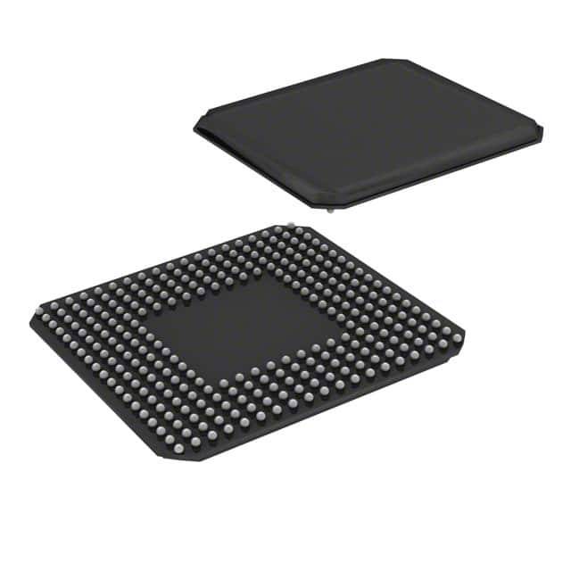
The XCS40XL-5CS280C comes in a compact package, ensuring easy integration into electronic systems. It is available in a surface-mount package, allowing for efficient assembly on printed circuit boards.
Essence
The essence of the XCS40XL-5CS280C lies in its ability to provide reconfigurable hardware, enabling users to implement complex digital designs with flexibility and efficiency.
Packaging/Quantity
The XCS40XL-5CS280C is typically packaged in reels or trays, depending on the manufacturer's specifications. The quantity per package may vary, but it is commonly available in quantities suitable for both prototyping and production purposes.
Specifications
- FPGA Family: Xilinx Spartan-XL
- Model: XCS40XL-5CS280C
- Logic Cells: 40,000
- Speed Grade: -5
- I/O Pins: 280
- Operating Voltage: 3.3V
- Package Type: CS280
Detailed Pin Configuration
The XCS40XL-5CS280C has 280 I/O pins, which can be configured for various purposes such as input, output, or bidirectional communication. The pin configuration is detailed in the product datasheet provided by the manufacturer.
Functional Features
- Configurable Logic Blocks (CLBs) for implementing custom logic functions
- Programmable interconnects for flexible routing of signals
- Dedicated hardware resources for arithmetic operations, memory interfaces, and communication protocols
- On-chip clock management circuitry for precise timing control
- Support for various I/O standards and voltage levels
Advantages and Disadvantages
Advantages
- Flexibility: The XCS40XL-5CS280C allows users to modify the functionality of the FPGA even after it has been manufactured, providing adaptability to changing requirements.
- High Performance: With a large number of logic cells and high-speed processing capabilities, the XCS40XL-5CS280C can handle complex digital designs efficiently.
- Power Efficiency: The FPGA is designed to minimize power consumption, making it suitable for applications with strict power constraints.
- Reliability: The robust design of the XCS40XL-5CS280C ensures reliable operation in demanding environments.
Disadvantages
- Complexity: Utilizing the full potential of an FPGA requires expertise in digital design and programming, which may pose a challenge for beginners or those unfamiliar with FPGA technology.
- Cost: FPGAs can be more expensive compared to other integrated circuits due to their advanced features and customization capabilities.
Working Principles
The XCS40XL-5CS280C operates based on the principles of reconfigurable hardware. It consists of configurable logic blocks (CLBs) that can be programmed to implement desired logic functions. These CLBs are interconnected through programmable interconnects, allowing for flexible routing of signals. By configuring the CLBs and interconnects, users can create custom digital circuits tailored to their specific application requirements.
Detailed Application Field Plans
The XCS40XL-5CS280C finds applications in various fields, including but not limited to:
- Telecommunications: Used in network equipment, routers, and switches for high-speed data processing and protocol handling.
- Industrial Automation: Employed in control systems, motor drives, and robotics for real-time control and signal processing.
- Aerospace and Defense: Utilized in radar systems, avionics, and military communication equipment for high-performance signal processing and encryption.
- Medical Devices: Integrated into medical imaging systems, patient monitoring devices, and laboratory equipment for data acquisition and processing.
- Automotive: Applied in advanced driver assistance systems (ADAS), infotainment systems, and engine control units (ECUs) for efficient data processing and control.
Detailed and Complete Alternative Models
- XCS10XL-4VQG100C
- XCS25XL-5TQG144C
- XCS50XL-6PQG240C
- XCS100XL-4FG256C
- XCS200XL-4BG256C
These alternative models offer varying capacities, I/O pin counts, and package options, providing users with a range of choices based on their specific requirements.
*
기술 솔루션에 XCS40XL-5CS280C 적용과 관련된 10가지 일반적인 질문과 답변을 나열하세요.
Sure! Here are 10 common questions and answers related to the application of XCS40XL-5CS280C in technical solutions:
Question: What is the XCS40XL-5CS280C FPGA used for?
Answer: The XCS40XL-5CS280C FPGA is a programmable logic device used for implementing digital circuits and systems.Question: What is the maximum number of logic cells available in the XCS40XL-5CS280C?
Answer: The XCS40XL-5CS280C has a maximum of 40,960 logic cells.Question: Can the XCS40XL-5CS280C be used for high-speed data processing applications?
Answer: Yes, the XCS40XL-5CS280C is capable of handling high-speed data processing due to its advanced architecture and high-performance features.Question: What is the maximum clock frequency supported by the XCS40XL-5CS280C?
Answer: The XCS40XL-5CS280C can support clock frequencies up to 280 MHz.Question: Is the XCS40XL-5CS280C suitable for embedded system designs?
Answer: Yes, the XCS40XL-5CS280C is commonly used in embedded system designs due to its flexibility and reconfigurability.Question: Can the XCS40XL-5CS280C interface with other components or peripherals?
Answer: Yes, the XCS40XL-5CS280C supports various interfaces such as UART, SPI, I2C, and Ethernet, allowing it to communicate with other components or peripherals.Question: What development tools are available for programming the XCS40XL-5CS280C?
Answer: Xilinx provides the Vivado Design Suite, which includes tools for designing, simulating, and programming the XCS40XL-5CS280C.Question: Can the XCS40XL-5CS280C be used in safety-critical applications?
Answer: Yes, the XCS40XL-5CS280C can be used in safety-critical applications as long as proper design and verification processes are followed.Question: What power supply voltage is required for the XCS40XL-5CS280C?
Answer: The XCS40XL-5CS280C operates at a core voltage of 1.2V and requires additional voltages for I/O banks.Question: Are there any specific temperature requirements for the XCS40XL-5CS280C?
Answer: The XCS40XL-5CS280C has an operating temperature range of -40°C to 100°C, making it suitable for a wide range of environments.
Please note that the answers provided here are general and may vary depending on specific application requirements.